 |
Electronic Components Datasheet Search |
|
|
Electronic Components Datasheet Search |
|
The question interval is too short.
Please try again in a few seconds.

Hello, Please ask a question about AS29F040-120TC Datasheet
# Example questions:
➢ What bus cycle operation is required to verify the programming status of a cell?
➢ What is the minimum time that must elapse between writing the sector erase command to multiple sectors to ensure they are all erased?
➢ What must be read to verify the write protect status of sectors, and what values on dq0 indicate a protected vs. unprotected sector?
| Part No. | AS29F040-120TC |
| Manufacturer | ALSC |
| Size | 341 Kbytes |
| Pages | 18 pages |
| Description | 5V 512K x 8 CMOS FLASH EEPROM |

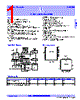






1. General Overview & Key Features
️· Type: Flash memory chip.
️· Functionality: Allows for byte-by-byte programming, sector erasing, and chip erasing.
️· No CPU Control Required: Much of the programming/erasing process is handled internally, reducing CPU overhead.
️· Data Polling: Allows the CPU to monitor the progress of programming/erasing operations.
2. Sector/Chip Erase Details
️· Sector Erase:
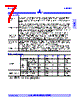
- Requires a 6-cycle process: two unlock write cycles, a setup command, two additional unlock write cycles, and the sector erase command (30h).
- The sector to be erased is identified by the address latched during the process.
- Multiple sectors can be erased sequentially, but timing is crucial – writes between sectors must be within 80 µs.
- The chip automatically programs all sectors with 0s before erasing.
- Can be interrupted by a falling edge on WE and must be restarted.
️· Chip Erase:
- Also a 6-cycle process.
- Erases the entire memory array, programming all cells to 0.
3. Programming Details
️· Byte-by-Byte Programming: Programming occurs byte-by-byte.
️· Unlock Write Cycles: Two unlock write cycles precede programming.
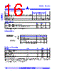
️· Data Polling: DQ7 and DQ6 are used for data polling to monitor the status of the programming process. DQ5 goes high if the programming time limit is exceeded.
️· Programming 0s to 1s: Requires an erase operation due to the chip's architecture.
4. Write Protection
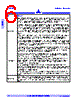
️· Verification: Write protection status of sectors is verified by reading address XXX02h. A '1' on DQ0 indicates a protected sector, and a '0' indicates an unprotected sector.
5. Command Sequence (General)
️· The datasheet has multiple 6-cycle command sequences for erase.
Key Terminology
️· WE (Write Enable): A signal used to trigger commands.
️· CE (Chip Enable): A signal that enables the chip.
️· DQ (Data Queue): The data lines for reading and writing.
️· DQ0-DQ7: Specific data lines used for polling and status.
️· XXX00h, XXX01h, XXX02h: Specific memory addresses used for retrieving MFG code, device code and write protection status respectively.
1. General Overview & Key Features
️· Type: Flash memory chip.
️· Functionality: Allows for byte-by-byte programming, sector erasing, and chip erasing.
️· No CPU Control Required: Much of the programming/erasing process is handled internally, reducing CPU overhead.
️· Data Polling: Allows the CPU to monitor the progress of programming/erasing operations.
2. Sector/Chip Erase Details
️· Sector Erase:
- Requires a 6-cycle process: two unlock write cycles, a setup command, two additional unlock write cycles, and the sector erase command (30h).
- The sector to be erased is identified by the address latched during the process.
- Multiple sectors can be erased sequentially, but timing is crucial – writes between sectors must be within 80 µs.
- The chip automatically programs all sectors with 0s before erasing.
- Can be interrupted by a falling edge on WE and must be restarted.
️· Chip Erase:
- Also a 6-cycle process.
- Erases the entire memory array, programming all cells to 0.
3. Programming Details
️· Byte-by-Byte Programming: Programming occurs byte-by-byte.
️· Unlock Write Cycles: Two unlock write cycles precede programming.
️· Data Polling: DQ7 and DQ6 are used for data polling to monitor the status of the programming process. DQ5 goes high if the programming time limit is exceeded.
️· Programming 0s to 1s: Requires an erase operation due to the chip's architecture.
4. Write Protection
️· Verification: Write protection status of sectors is verified by reading address XXX02h. A '1' on DQ0 indicates a protected sector, and a '0' indicates an unprotected sector.
5. Command Sequence (General)
️· The datasheet has multiple 6-cycle command sequences for erase.
Key Terminology
️· WE (Write Enable): A signal used to trigger commands.
️· CE (Chip Enable): A signal that enables the chip.
️· DQ (Data Queue): The data lines for reading and writing.
️· DQ0-DQ7: Specific data lines used for polling and status.
️· XXX00h, XXX01h, XXX02h: Specific memory addresses used for retrieving MFG code, device code and write protection status respectively.
| Part No. | AS29F040-120TC |
| Manufacturer | ALSC |
| Size | 341 Kbytes |
| Pages | 18 pages |
| Description | 5V 512K x 8 CMOS FLASH EEPROM |
| Does ALLDATASHEET help your business so far? [ DONATE ] |
About Alldatasheet | Advertisement | Contact us | Privacy Policy | Link to Datasheet | Link Exchange | Manufacturer List All Rights Reserved©Alldatasheet.com |
| Russian : Alldatasheetru.com | Korean : Alldatasheet.co.kr | Spanish : Alldatasheet.es | French : Alldatasheet.fr | Italian : Alldatasheetit.com Portuguese : Alldatasheetpt.com | Polish : Alldatasheet.pl | Vietnamese : Alldatasheet.vn Indian : Alldatasheet.in | Mexican : Alldatasheet.com.mx | British : Alldatasheet.co.uk | New Zealand : Alldatasheet.co.nz |
|
Family Site : ic2ic.com |
icmetro.com |
 British ▼
  English
 Chinese
 German
 Japanese
 Russian
 Korean
 Spanish
 French
 Italian
 Portuguese
 Polish
 Vietnamese
 Indian
 Mexican
 New Zealand