 |
Electronic Components Datasheet Search |
|
|
Electronic Components Datasheet Search |
|
The question interval is too short.
Please try again in a few seconds.

Hello, Please ask a question about XC25BS5_002 Datasheet
# Example questions:
➢ What are the recommended bypass capacitor and matching resistor placements to ensure optimal performance and minimize unwanted radiation?
➢ Under what conditions would each of these values be relevant or measured?
➢ What specific types of applications are explicitly *not* recommended for devices utilizing this ic, and why?
| Part No. | XC25BS5_002 |
| Manufacturer | TOREX |
| Size | 477 Kbytes |
| Pages | 10 pages |
| Description | PLL Clock Generator ICs with Built-In Divider/Multiplier Circuits(For Low Frequency Range) |

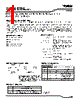






# XC25BS5 Series PLL Clock Generator ICs
## GENERAL DESCRIPTION
The XC25BS5 series are high frequency, low power consumption PLL clock generator ICs with divider and multiplier circuits. They offer selectable divider (1, 3-2047) and multiplier (6-2047) ratios. Output frequency (Q0) ranges from 3MHz to 30MHz and is determined by the reference clock (fCLKin) multiplied by N/M. Q1 output is selectable (reference frequency, frequency/2, GND, comparative frequency). Standby mode is supported for low power consumption.
## APPLICATIONS
️· Crystal oscillation modules
️· Personal computers
️· PDAs
️· Portable audio systems
️· Various system clocks
## FEATURES
️· Output Frequency: 3MHz ~ 30MHz
️· Input Frequency: 12kHz ~ 35MHz
️· Divider Ratio (M): 1, 3 ~ 2047
️· Multiplier Ratio (N): 6 ~ 2047
️· Operating Voltage: 2.97V ~ 5.5V
️· Package: SOT-26, USP-6B
️· Low Power Consumption: CMOS with standby function
️· Comparative Frequency: 12kHz ~ 500kHz
## PIN CONFIGURATION
| PIN # (SOT-26/USP-6B) | PIN NAME | FUNCTION |
|---|---|---|
| 1/3 | Q0 | PLL Output |
| 2/2 | VSS | GND |
| 3/1 | CE | Chip Enable |
| 4/6 | Q1 | Reference Oscillation, Frequency/2, GND, Comparative Frequency Output |
| 5/5 | VDD | Power Supply |
| 6/4 | CLKin | Reference Clock Input |
# XC25BS5 Series PLL Clock Generator ICs
## GENERAL DESCRIPTION
The XC25BS5 series are high frequency, low power consumption PLL clock generator ICs with divider and multiplier circuits. They offer selectable divider (1, 3-2047) and multiplier (6-2047) ratios. Output frequency (Q0) ranges from 3MHz to 30MHz and is determined by the reference clock (fCLKin) multiplied by N/M. Q1 output is selectable (reference frequency, frequency/2, GND, comparative frequency). Standby mode is supported for low power consumption.
## APPLICATIONS
️· Crystal oscillation modules
️· Personal computers
️· PDAs
️· Portable audio systems
️· Various system clocks
## FEATURES
️· Output Frequency: 3MHz ~ 30MHz
️· Input Frequency: 12kHz ~ 35MHz
️· Divider Ratio (M): 1, 3 ~ 2047
️· Multiplier Ratio (N): 6 ~ 2047
️· Operating Voltage: 2.97V ~ 5.5V
️· Package: SOT-26, USP-6B
️· Low Power Consumption: CMOS with standby function
️· Comparative Frequency: 12kHz ~ 500kHz
## PIN CONFIGURATION
| PIN # (SOT-26/USP-6B) | PIN NAME | FUNCTION |
|---|---|---|
| 1/3 | Q0 | PLL Output |
| 2/2 | VSS | GND |
| 3/1 | CE | Chip Enable |
| 4/6 | Q1 | Reference Oscillation, Frequency/2, GND, Comparative Frequency Output |
| 5/5 | VDD | Power Supply |
| 6/4 | CLKin | Reference Clock Input |
| Part No. | XC25BS5_002 |
| Manufacturer | TOREX |
| Size | 477 Kbytes |
| Pages | 10 pages |
| Description | PLL Clock Generator ICs with Built-In Divider/Multiplier Circuits(For Low Frequency Range) |
| Does ALLDATASHEET help your business so far? [ DONATE ] |
About Alldatasheet | Advertisement | Contact us | Privacy Policy | Link to Datasheet | Link Exchange | Manufacturer List All Rights Reserved©Alldatasheet.com |
| Russian : Alldatasheetru.com | Korean : Alldatasheet.co.kr | Spanish : Alldatasheet.es | French : Alldatasheet.fr | Italian : Alldatasheetit.com Portuguese : Alldatasheetpt.com | Polish : Alldatasheet.pl | Vietnamese : Alldatasheet.vn Indian : Alldatasheet.in | Mexican : Alldatasheet.com.mx | British : Alldatasheet.co.uk | New Zealand : Alldatasheet.co.nz |
|
Family Site : ic2ic.com |
icmetro.com |
 British ▼
  English
 Chinese
 German
 Japanese
 Russian
 Korean
 Spanish
 French
 Italian
 Portuguese
 Polish
 Vietnamese
 Indian
 Mexican
 New Zealand