 |
Electronic Components Datasheet Search |
|
|
Electronic Components Datasheet Search |
|
The question interval is too short.
Please try again in a few seconds.

Hello, Please ask a question about ATA6662_09 Datasheet
# Example questions:
➢ What happens to the lin bus if the device loses its connection to ground, and what is the maximum allowable leakage current in this scenario?
➢ What are the minimum and maximum voltage levels for the wake pin, and what is the typical range for the wake pull-up current?
➢ What is the typical range for the txd pull-down resistor value, and what type of testing is performed on this parameter?
| Part No. | ATA6662_09 |
| Manufacturer | ATMEL |
| Size | 533 Kbytes |
| Pages | 18 pages |
| Description | LIN Transceiver |

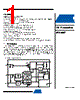


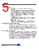


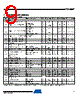


1. General Information & Operating Conditions:
️· Supply Voltage (VS): 5V to 27V
️· Operating Temperature (Tj): -40°C to +150°C
️· Type classification: A= 100% tested, B = 100% correlation tested, C = Characterized on samples, D = Design parameter
2. Pin Functions and Electrical Characteristics (Values are min/typ/max unless stated):
(a) Power Supply & General Inputs/Outputs
️· EN (Enable Input):
- Low-level Input Voltage (VENL): -0.3V to +0.8V
- High-level Input Voltage (VENH): 2V to 5.5V
- Pull-down Resistor (REN): 125kΩ to 250kΩ to 600kΩ
- Low-Level Input Current (IEN): -3µA to +3µA
️· WAKE Pin:
- High-level Input Voltage (VWAKEH): VS – 1V to VS + 0.3V
- Low-level Input Voltage (VWAKEL): -1V to VS – 3.3V
- Wake Pull-up Current (IWAKE): -30µA to -10µA
- High-level Leakage Current: -5µA to +5µA
️· TXD (Transmit Data Input):
- Low-level Voltage Input (VTXDL): -0.3V to +0.8V
- High-level Voltage Input (VTXDH): 2V to 5.5V
- Pull-down Resistor (RTXD): 125kΩ to 250kΩ to 600kΩ
- Low-level Leakage Current (ITXD_leak): -3µA to +3µA
- Low-level output sink current (ITXD): 1.3mA to 2.5mA to 8mA
️· LIN Bus Driver (Pin 6):
- Dominant Voltage (VBUSdom_DRV_LoSUP): 0.6V (for 7V supply), dependent on supply voltage
- Driver dominant voltage (V_HiSUP): 0.8V(for 18V supply), dependent on supply voltage
- Pull-up Resistor (RLIN): 20kΩ to 30kΩ to 60kΩ
- LIN current limitation (IBUS_LIM): 40mA to 120mA to 200mA
- Leakage current (IBUS_PAS_dom): -1mA to +0.5mA to 10mA
(b) More LIN Bus Driver Specifications:
️· Dominant Output Voltage: 0.9 x VS to VS (depends on supply voltage)
️· Input leakage current at receiver: -1µA to +0.5µA to 10µA
(c) RXD (Receive Data Input):
️· Low-level Output Sink Current: 1.3mA to 2.5mA to 8mA
️· Saturation Voltage: 0.0V to 0.4V
️· Leakage Current: -3µA to +3µA
️· ESD zener diode: 5.8V
(d) INH (Inhibit Output):
️· High-level voltage: VS – 3V to VS
️· Leakage current: -3µA to +3µA
3. Special Operating Conditions & Protection:
️· Battery Loss/Ground Loss Protection: The LIN bus needs to remain operational even if the battery is disconnected or the ground is lost. (See IBUS_NO_bat and IBUS_NO_gnd)
️· ESD Protection Zener diodes are incorporated into RXD.
IMPORTANT NOTES AND CAVEATS:
️· "Type" Designations: Pay close attention to the "Type" (A, B, C, D) designations for each electrical characteristic. This indicates the level of testing and reliability associated with that value.
️· Supply Voltage Dependence: Many characteristics, especially those related to the LIN bus driver voltages (e.g., V_HiSUP, V_LoSUP), *depend on the supply voltage (VS)*. The provided values are for specific supply voltages and will change with different voltages.
️· Refer to the Full Datasheet: This is a highly condensed summary. ALWAYS refer to the full ATA6662 datasheet for complete details, conditions, and applicable diagrams. There are many more parameters and conditions not covered here.
️· Safety and Application Notes: Datasheets often contain important safety information and application notes. Be sure to read those sections.
1. General Information & Operating Conditions:
️· Supply Voltage (VS): 5V to 27V
️· Operating Temperature (Tj): -40°C to +150°C
️· Type classification: A= 100% tested, B = 100% correlation tested, C = Characterized on samples, D = Design parameter
2. Pin Functions and Electrical Characteristics (Values are min/typ/max unless stated):
(a) Power Supply & General Inputs/Outputs
️· EN (Enable Input):
- Low-level Input Voltage (VENL): -0.3V to +0.8V
- High-level Input Voltage (VENH): 2V to 5.5V
- Pull-down Resistor (REN): 125kΩ to 250kΩ to 600kΩ
- Low-Level Input Current (IEN): -3µA to +3µA
️· WAKE Pin:
- High-level Input Voltage (VWAKEH): VS – 1V to VS + 0.3V
- Low-level Input Voltage (VWAKEL): -1V to VS – 3.3V
- Wake Pull-up Current (IWAKE): -30µA to -10µA
- High-level Leakage Current: -5µA to +5µA
️· TXD (Transmit Data Input):
- Low-level Voltage Input (VTXDL): -0.3V to +0.8V
- High-level Voltage Input (VTXDH): 2V to 5.5V
- Pull-down Resistor (RTXD): 125kΩ to 250kΩ to 600kΩ
- Low-level Leakage Current (ITXD_leak): -3µA to +3µA
- Low-level output sink current (ITXD): 1.3mA to 2.5mA to 8mA
️· LIN Bus Driver (Pin 6):
- Dominant Voltage (VBUSdom_DRV_LoSUP): 0.6V (for 7V supply), dependent on supply voltage
- Driver dominant voltage (V_HiSUP): 0.8V(for 18V supply), dependent on supply voltage
- Pull-up Resistor (RLIN): 20kΩ to 30kΩ to 60kΩ
- LIN current limitation (IBUS_LIM): 40mA to 120mA to 200mA
- Leakage current (IBUS_PAS_dom): -1mA to +0.5mA to 10mA
(b) More LIN Bus Driver Specifications:
️· Dominant Output Voltage: 0.9 x VS to VS (depends on supply voltage)
️· Input leakage current at receiver: -1µA to +0.5µA to 10µA
(c) RXD (Receive Data Input):
️· Low-level Output Sink Current: 1.3mA to 2.5mA to 8mA
️· Saturation Voltage: 0.0V to 0.4V
️· Leakage Current: -3µA to +3µA
️· ESD zener diode: 5.8V
(d) INH (Inhibit Output):
️· High-level voltage: VS – 3V to VS
️· Leakage current: -3µA to +3µA
3. Special Operating Conditions & Protection:
️· Battery Loss/Ground Loss Protection: The LIN bus needs to remain operational even if the battery is disconnected or the ground is lost. (See IBUS_NO_bat and IBUS_NO_gnd)
️· ESD Protection Zener diodes are incorporated into RXD.
IMPORTANT NOTES AND CAVEATS:
️· "Type" Designations: Pay close attention to the "Type" (A, B, C, D) designations for each electrical characteristic. This indicates the level of testing and reliability associated with that value.
️· Supply Voltage Dependence: Many characteristics, especially those related to the LIN bus driver voltages (e.g., V_HiSUP, V_LoSUP), *depend on the supply voltage (VS)*. The provided values are for specific supply voltages and will change with different voltages.
️· Refer to the Full Datasheet: This is a highly condensed summary. ALWAYS refer to the full ATA6662 datasheet for complete details, conditions, and applicable diagrams. There are many more parameters and conditions not covered here.
️· Safety and Application Notes: Datasheets often contain important safety information and application notes. Be sure to read those sections.
| Part No. | ATA6662_09 |
| Manufacturer | ATMEL |
| Size | 533 Kbytes |
| Pages | 18 pages |
| Description | LIN Transceiver |
| Does ALLDATASHEET help your business so far? [ DONATE ] |
About Alldatasheet | Advertisement | Contact us | Privacy Policy | Link to Datasheet | Link Exchange | Manufacturer List All Rights Reserved©Alldatasheet.com |
| Russian : Alldatasheetru.com | Korean : Alldatasheet.co.kr | Spanish : Alldatasheet.es | French : Alldatasheet.fr | Italian : Alldatasheetit.com Portuguese : Alldatasheetpt.com | Polish : Alldatasheet.pl | Vietnamese : Alldatasheet.vn Indian : Alldatasheet.in | Mexican : Alldatasheet.com.mx | British : Alldatasheet.co.uk | New Zealand : Alldatasheet.co.nz |
|
Family Site : ic2ic.com |
icmetro.com |
 British ▼
  English
 Chinese
 German
 Japanese
 Russian
 Korean
 Spanish
 French
 Italian
 Portuguese
 Polish
 Vietnamese
 Indian
 Mexican
 New Zealand