 |
Electronic Components Datasheet Search |
|
|
Electronic Components Datasheet Search |
|
The question interval is too short.
Please try again in a few seconds.

Hello, Please ask a question about OP4017B Datasheet
# Example questions:
➢ What is the typical operating voltage (vcc) range for the op4017b, and what is the recommended value for optimal performance as specified in the datasheet?
➢ What factors are included in all specifications unless otherwise noted? list at least three.
➢ What does this caution indicate, and what action might be required before exporting this device?
| Part No. | OP4017B |
| Manufacturer | MURATA |
| Size | 71 Kbytes |
| Pages | 2 pages |
| Description | 777.60 MHz Optical Timing Clock |

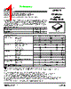


1. Device Identification and Purpose
️· Device: RF Monolithics OP4017B
️· Type: Voltage-Controlled Crystal Oscillator (VCXO) or similar frequency generation device. Likely a precision oscillator providing a stable clock signal.
️· Frequency: Operates at 7 MHz (as indicated in the title)
️· Application: Designed for applications needing precise timing, likely in telecommunications, data transmission, or optical networking systems (especially where the term "optical" is often used).
2. Key Specifications & Performance
️· Supply Voltage (VCC): 3.3V or 5.0V (Nominal 3.13V)
️· Power Consumption (ICC): 70 mA (maximum)
️· Operating Temperature Range: -40°C to +85°C
️· Tuning Input: A voltage applied to the Tuning Input changes the output frequency. The tuning range is not explicitly given, but it’s implied.
️· Phase Noise: Very low phase noise, critical for maintaining signal integrity in sensitive systems. Specific dBc/Hz values are listed in the table.
️· Jitter: Low jitter. Specific values are listed in the table.
️· Output DC Resistance: 50 Ohms.
️· Dimensions: Detailed mechanical dimensions are provided in a table (A-N) with both millimeters and inches.
3. Important Notes and Cautions
️· Electrostatic Discharge (ESD) Sensitivity: The device is extremely sensitive to ESD. Strict ESD precautions must be followed during handling and assembly (highlighted by the CAUTION).
️· Export Restrictions: Export of the device requires approval from the U.S. Department of Commerce (COCOM CAUTION).
️· Specifications are Subject to Change: The manufacturer reserves the right to modify the specifications without notice.
️· Optimized PCB Design: The optimum land pattern design for the PCB is critical for optimal performance.
4. Key Features & Benefits (Implied)
️· High Frequency Stability: The VCXO provides a very stable and accurate frequency output.
️· Low Noise: Excellent phase noise characteristics.
️· Adjustable Frequency: The Tuning Input allows for frequency adjustment.
️· Compact Size: The dimensions are relatively small, enabling integration into various systems.
️· Wide Operating Temperature Range: Can operate reliably in a wide range of environmental conditions.
5. Documentation & Support
️· Manufacturer: RF Monolithics (now part of Qorvo)
️· Website: [www.RFM.com](http://www.RFM.com) (website may be archived, as RF Monolithics was acquired)
️· Contact: info@rfm.com (email address may be archived)
️· Patents: Covered by several U.S. patents (listed).
1. Device Identification and Purpose
️· Device: RF Monolithics OP4017B
️· Type: Voltage-Controlled Crystal Oscillator (VCXO) or similar frequency generation device. Likely a precision oscillator providing a stable clock signal.
️· Frequency: Operates at 7 MHz (as indicated in the title)
️· Application: Designed for applications needing precise timing, likely in telecommunications, data transmission, or optical networking systems (especially where the term "optical" is often used).
2. Key Specifications & Performance
️· Supply Voltage (VCC): 3.3V or 5.0V (Nominal 3.13V)
️· Power Consumption (ICC): 70 mA (maximum)
️· Operating Temperature Range: -40°C to +85°C
️· Tuning Input: A voltage applied to the Tuning Input changes the output frequency. The tuning range is not explicitly given, but it’s implied.
️· Phase Noise: Very low phase noise, critical for maintaining signal integrity in sensitive systems. Specific dBc/Hz values are listed in the table.
️· Jitter: Low jitter. Specific values are listed in the table.
️· Output DC Resistance: 50 Ohms.
️· Dimensions: Detailed mechanical dimensions are provided in a table (A-N) with both millimeters and inches.
3. Important Notes and Cautions
️· Electrostatic Discharge (ESD) Sensitivity: The device is extremely sensitive to ESD. Strict ESD precautions must be followed during handling and assembly (highlighted by the CAUTION).
️· Export Restrictions: Export of the device requires approval from the U.S. Department of Commerce (COCOM CAUTION).
️· Specifications are Subject to Change: The manufacturer reserves the right to modify the specifications without notice.
️· Optimized PCB Design: The optimum land pattern design for the PCB is critical for optimal performance.
4. Key Features & Benefits (Implied)
️· High Frequency Stability: The VCXO provides a very stable and accurate frequency output.
️· Low Noise: Excellent phase noise characteristics.
️· Adjustable Frequency: The Tuning Input allows for frequency adjustment.
️· Compact Size: The dimensions are relatively small, enabling integration into various systems.
️· Wide Operating Temperature Range: Can operate reliably in a wide range of environmental conditions.
5. Documentation & Support
️· Manufacturer: RF Monolithics (now part of Qorvo)
️· Website: [www.RFM.com](http://www.RFM.com) (website may be archived, as RF Monolithics was acquired)
️· Contact: info@rfm.com (email address may be archived)
️· Patents: Covered by several U.S. patents (listed).
| Part No. | OP4017B |
| Manufacturer | MURATA |
| Size | 71 Kbytes |
| Pages | 2 pages |
| Description | 777.60 MHz Optical Timing Clock |
| Does ALLDATASHEET help your business so far? [ DONATE ] |
About Alldatasheet | Advertisement | Contact us | Privacy Policy | Link to Datasheet | Link Exchange | Manufacturer List All Rights Reserved©Alldatasheet.com |
| Russian : Alldatasheetru.com | Korean : Alldatasheet.co.kr | Spanish : Alldatasheet.es | French : Alldatasheet.fr | Italian : Alldatasheetit.com Portuguese : Alldatasheetpt.com | Polish : Alldatasheet.pl | Vietnamese : Alldatasheet.vn Indian : Alldatasheet.in | Mexican : Alldatasheet.com.mx | British : Alldatasheet.co.uk | New Zealand : Alldatasheet.co.nz |
|
Family Site : ic2ic.com |
icmetro.com |
 British ▼
  English
 Chinese
 German
 Japanese
 Russian
 Korean
 Spanish
 French
 Italian
 Portuguese
 Polish
 Vietnamese
 Indian
 Mexican
 New Zealand