|
Electronic Components Datasheet Search |
|
|
Electronic Components Datasheet Search |
|
H8SX/1663 Datasheet(PDF) 964 Page - Renesas Technology Corp |
|
|
|||||||||||||||||||||||||||||
H8SX/1663 Datasheet(HTML) 964 Page - Renesas Technology Corp |
|
|
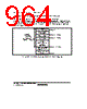
964 / 1158 page 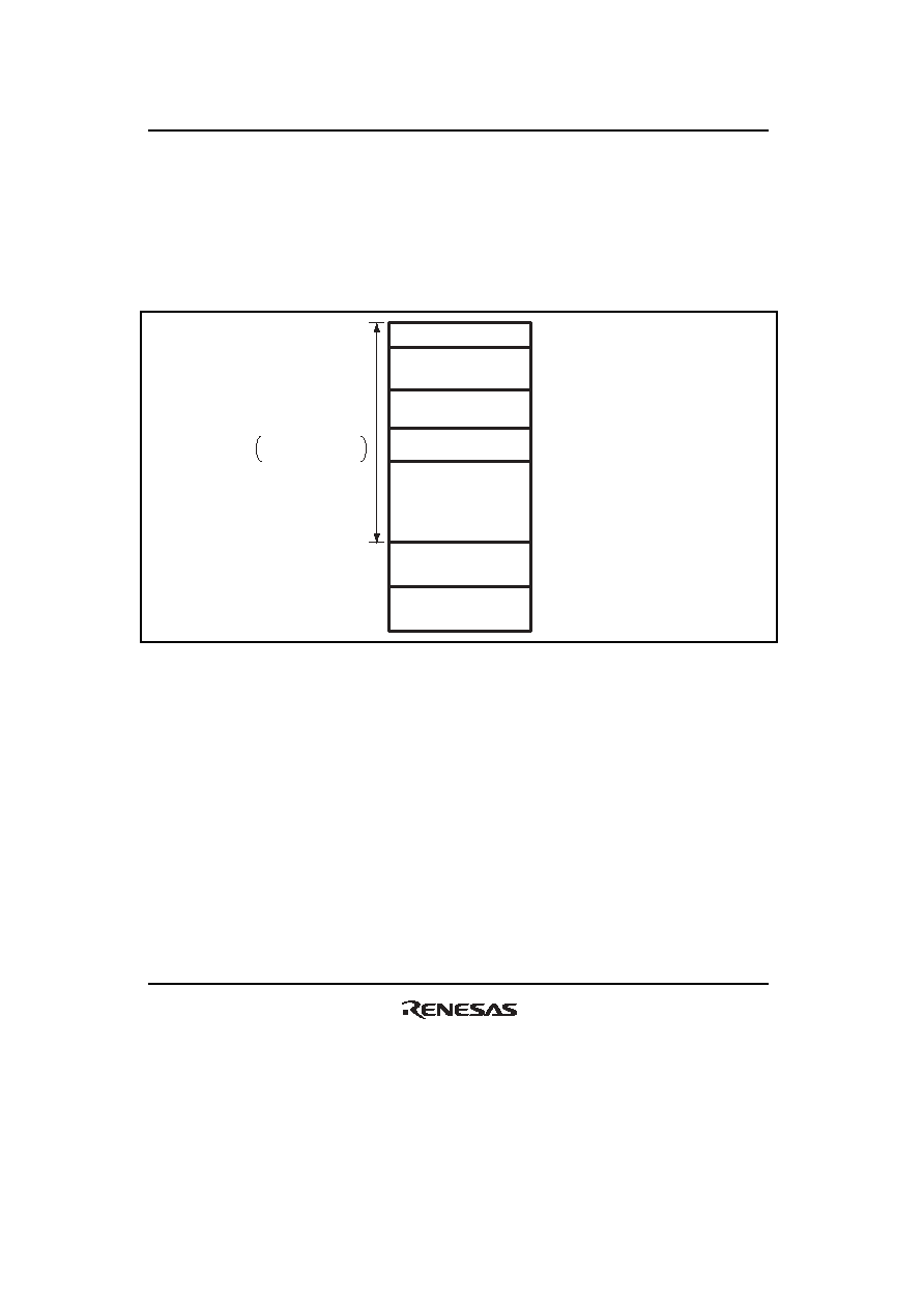 Section 21 Flash Memory (0.18- µm F-ZTAT Version) Rev.1.00 Jun. 07, 2006 Page 912 of 1102 REJ09B0294-0100 (1) On-Chip RAM Address Map when Programming/Erasing is Executed Parts of the procedure program that is made by the user, like download request, programming/erasing procedure, and decision of the result, must be executed in the on-chip RAM. Since the on-chip program to be downloaded is embedded in the on-chip RAM, make sure the on- chip program and procedure program do not overlap. Figure 21.12 shows the area of the on-chip program to be downloaded. H'FFBFFF Programming/erasing program entry System use area (15 bytes) DPFR (Return value: 1 byte) FTDAR setting FTDAR setting + 32 bytes FTDAR setting + 16 bytes Initialization program entry Initialization + programming program or Initialization + erasing program RAM emulation area or area that can be used by user Area that can be used by user Area to be downloaded (size: 4 kbytes) Unusable area during programming/erasing FTDAR setting + 4 kbytes Figure 21.12 RAM Map when Programming/Erasing is Executed |
|
Link URL |
| Does ALLDATASHEET help your business so far? [ DONATE ] |
About Alldatasheet | Advertisement | Contact us | Privacy Policy | Link to Datasheet | Link Exchange | Manufacturer List All Rights Reserved©Alldatasheet.com |
| Russian : Alldatasheetru.com | Korean : Alldatasheet.co.kr | Spanish : Alldatasheet.es | French : Alldatasheet.fr | Italian : Alldatasheetit.com Portuguese : Alldatasheetpt.com | Polish : Alldatasheet.pl | Vietnamese : Alldatasheet.vn Indian : Alldatasheet.in | Mexican : Alldatasheet.com.mx | British : Alldatasheet.co.uk | New Zealand : Alldatasheet.co.nz |
|
Family Site : ic2ic.com |
icmetro.com |
 British ▼
 English
 Chinese
 German
 Japanese
 Russian
 Korean
 Spanish
 French
 Italian
 Portuguese
 Polish
 Vietnamese
 Indian
 Mexican
 British
 New Zealand