 |
Electronic Components Datasheet Search |
|
|
Electronic Components Datasheet Search |
|
EM357-RTR Datasheet(PDF) 123 Page - List of Unclassifed Manufacturers |
|
|
|||||||||||||||||||||||||||||
EM357-RTR Datasheet(HTML) 123 Page - List of Unclassifed Manufacturers |
|
|
123 / 240 page 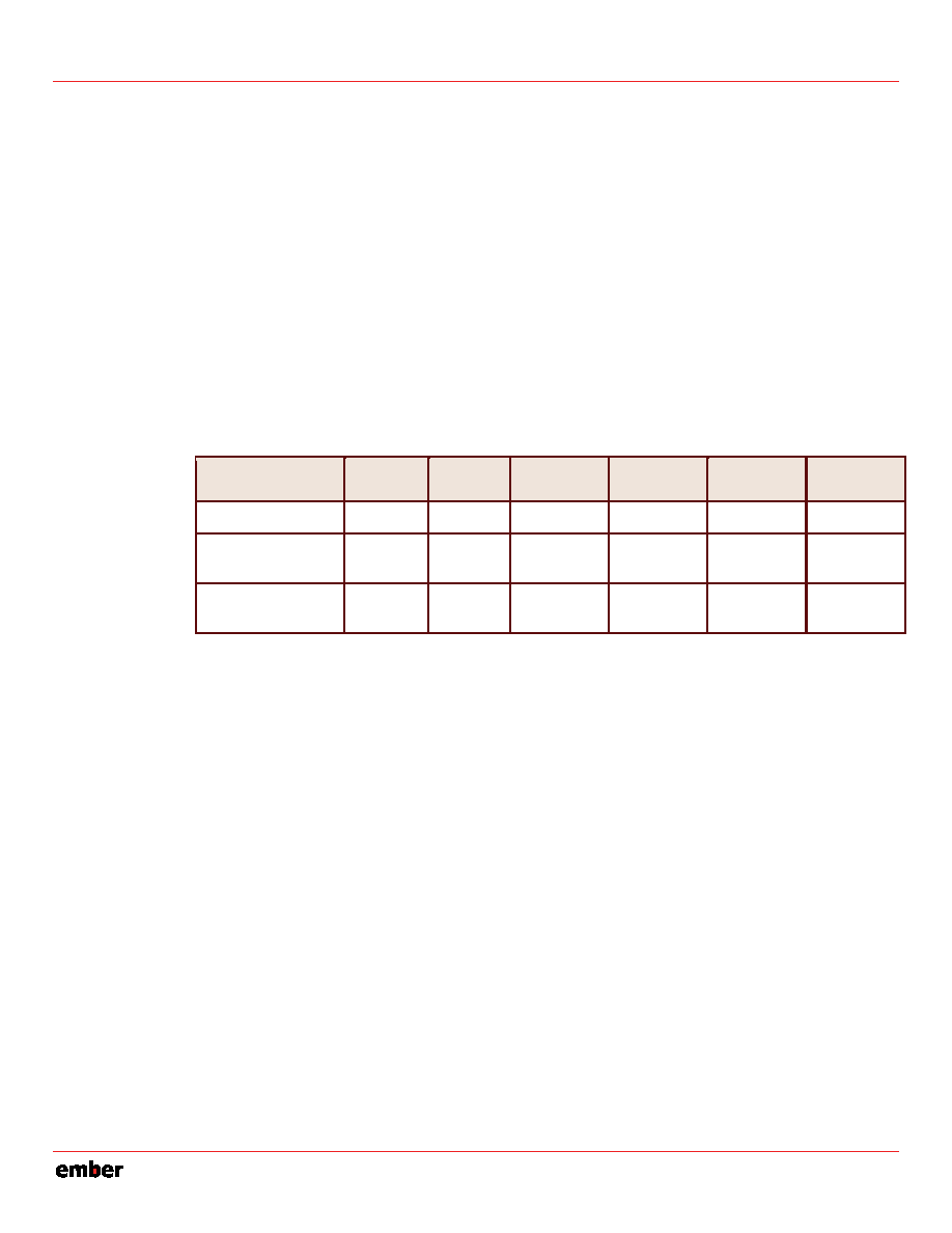 EM351 / EM357 9.2 GPIO Usage The timers can optionally use GPIOs in the PA and PB ports for external inputs or outputs. As with all EM35x digital inputs, a GPIO used as a timer input can be shared with other uses of the same pin. Available timer inputs include an external timer clock, a clock mask, and four input channels. Any GPIO used as a timer output must be configured as an alternate output and is controlled only by the timer. Many of the GPIOs that can be assigned as timer outputs can also be used by another on-chip peripheral such as a serial controller. Using a GPIO as a timer output takes precedence over another peripheral function, as long as the channel is configured as an output in the TIMx_CCMR1 register and is enabled in the TIMx_CCER register. The GPIOs that can be used by Timer 1 are fixed, but the GPIOs that can be used as Timer 2 channels can be mapped to either of two pins, as shown in Table 9-1. The Timer 2 Option Register (TIM2_OR) has four single bit fields (TIM_REMAPCy) that control whether a Timer 2 channel is mapped to its default GPIO in port PA, or remapped to a GPIO in PB. Table 9-1 specifies the pins that may be assigned to Timer 1 and Timer 2 functions. Table 9-1. Timer GPIO Usage Signal (direction) TIMxC1 (in or out) TIMxC2 (in or out) TIMxC3 (in or out) TIMxC4 (in or out) TIMxCLK (in) TIMxMSK (in) Timer 1 PB6 PB7 PA6 PA7 PB0 PB5 Timer 2 (TIM_REMAPCy = 0) PA0 PA3 PA1 PA2 PB5 PB0 Timer 2 (TIM_REMAPCy = 1) PB1 PB2 PB3 PB4 PB5 PB0 The TIMxCLK and TIMxMSK inputs can be used only in the external clock modes: refer to the External Clock Source Mode 1 and External Clock Source Mode 2 sections for details concerning their use. 9.3 Timer Functional Description 9.3.1 Time-Base Unit The main block of the general purpose timer is a 16-bit counter with its related auto-reload register. The counter can count up, down, or alternate up and down. The counter clock can be divided by a prescaler. The counter, the auto-reload register, and the prescaler register can be written to or read by software. This is true even when the counter is running. The time-base unit includes: Counter Register (TIMx_CNT) Prescaler Register (TIMx_PSC): Auto-Reload Register (TIMx_ARR) Some timer registers cannot be directly accessed by software, which instead reads and writes a “buffer register”. The internal registers actually used for timer operations are called “shadow registers”. The auto-reload register is buffered. Writing to or reading from the auto-reload register accesses the buffer register. The contents of the buffer register are transferred into the shadow register permanently or at each 9-3 120-035X-000D Preliminary |
|
Link URL |
| Does ALLDATASHEET help your business so far? [ DONATE ] |
About Alldatasheet | Advertisement | Contact us | Privacy Policy | Link to Datasheet | Link Exchange | Manufacturer List All Rights Reserved©Alldatasheet.com |
| Russian : Alldatasheetru.com | Korean : Alldatasheet.co.kr | Spanish : Alldatasheet.es | French : Alldatasheet.fr | Italian : Alldatasheetit.com Portuguese : Alldatasheetpt.com | Polish : Alldatasheet.pl | Vietnamese : Alldatasheet.vn Indian : Alldatasheet.in | Mexican : Alldatasheet.com.mx | British : Alldatasheet.co.uk | New Zealand : Alldatasheet.co.nz |
|
Family Site : ic2ic.com |
icmetro.com |
 British ▼
 English
 Chinese
 German
 Japanese
 Russian
 Korean
 Spanish
 French
 Italian
 Portuguese
 Polish
 Vietnamese
 Indian
 Mexican
 British
 New Zealand


