 |
Electronic Components Datasheet Search |
|
|
Electronic Components Datasheet Search |
|
EM357-RTR Datasheet(PDF) 136 Page - List of Unclassifed Manufacturers |
|
|
|||||||||||||||||||||||||||||
EM357-RTR Datasheet(HTML) 136 Page - List of Unclassifed Manufacturers |
|
|
136 / 240 page 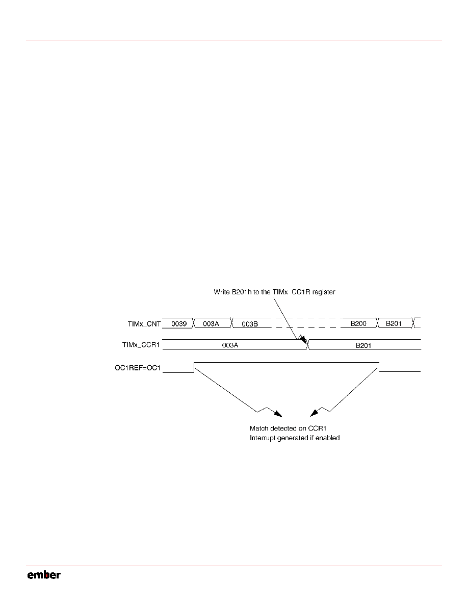 EM351 / EM357 Sets a flag in the interrupt flag register (the INT_TIMCCyIF bit in the INT_TIMxFLAG register). Generates an interrupt if the corresponding interrupt mask is set (the TIM_CCyIF bit in the INT_TIMxCFG register). The TIMx_CCRy registers can be programmed with or without buffer registers using the TIM_OCyBE bit in the TIMx_CCMR1 register. In output compare mode, the UEV has no effect on OCyREF or the OCy output. The timing resolution is one count of the counter. Output compare mode can also be used to output a single pulse (in one pulse mode). Procedure: 1. Select the counter clock (internal, external, and prescaler). 2. Write the desired data in the TIMx_ARR and TIMx_CCRy registers. 3. Set the INT_TIMCCyIF bit in INT_TIMxCFG if an interrupt request is to be generated. 4. Select the output mode. For example, you must write TIM_OCyM = 011, TIM_OCyBE = 0, TIM_CCyP = 0 and TIM_CCyE = 1 to toggle the OCy output pin when TIMx_CNT matches TIMx_CCRy, TIMx_CCRy buffer is not used, OCy is enabled and active high. 5. Enable the counter: Set the TIM_CEN bit in the TIMx_CR1 register. To control the output waveform, software can update the TIMx_CCRy register at any time, provided that the buffer register is not enabled (TIM_OCyBE = 0). Otherwise TIMx_CCRy shadow register is updated only at the next UEV. An example is given in Figure 9-21. Figure 9-21. Output Compare Mode, Toggle on OC1 9.3.9 PWM Mode Pulse width modulation mode allows you to generate a signal with a frequency determined by the value of the TIMx_ARR register, and a duty cycle determined by the value of the TIMx_CCRy register. PWM mode can be selected independently on each channel (one PWM per OCy output) by writing 110 (PWM mode 1) or 111 (PWM mode 2) in the TIM_OCyM bits in the TIMx_CCMR1 register. The corresponding buffer register must be enabled by setting the TIM_OCyBE bit in the TIMx_CCMR1 register. Finally, in up-counting or center-aligned mode the auto-reload buffer register must be enabled by setting the TIM_ARBE bit in the TIMx_CR1 register. 9-16 120-035X-000D Preliminary |
|
Link URL |
| Does ALLDATASHEET help your business so far? [ DONATE ] |
About Alldatasheet | Advertisement | Contact us | Privacy Policy | Link to Datasheet | Link Exchange | Manufacturer List All Rights Reserved©Alldatasheet.com |
| Russian : Alldatasheetru.com | Korean : Alldatasheet.co.kr | Spanish : Alldatasheet.es | French : Alldatasheet.fr | Italian : Alldatasheetit.com Portuguese : Alldatasheetpt.com | Polish : Alldatasheet.pl | Vietnamese : Alldatasheet.vn Indian : Alldatasheet.in | Mexican : Alldatasheet.com.mx | British : Alldatasheet.co.uk | New Zealand : Alldatasheet.co.nz |
|
Family Site : ic2ic.com |
icmetro.com |
 British ▼
 English
 Chinese
 German
 Japanese
 Russian
 Korean
 Spanish
 French
 Italian
 Portuguese
 Polish
 Vietnamese
 Indian
 Mexican
 British
 New Zealand


