 |
Electronic Components Datasheet Search |
|
|
Electronic Components Datasheet Search |
|
The question interval is too short.
Please try again in a few seconds.

Hello, Please ask a question about OP4017B1 Datasheet
# Example questions:
➢ What is the definition of 'symmetry' as it relates to the output signals, and how is it measured?
➢ What is the typical operating voltage (vcc) for the op4017b, and what is the operating temperature range?
➢ What does this caution signify regarding the export of this device?
| Part No. | OP4017B1 |
| Manufacturer | MURATA |
| Size | 71 Kbytes |
| Pages | 2 pages |
| Description | 777.60 MHz Optical Timing Clock |

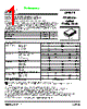

Okay, here's a breakdown of the key information from the provided document about the RF Monolithics OP4017B:
1. General Description:
️· Type: Voltage-Controlled Crystal Oscillator (VCXO) / Voltage-Controlled Oscillator (VCO). Essentially a precise clock generator.
️· Frequency: 77.112 MHz
️· Purpose: Designed for optical communication systems (like fiber optics) and other applications requiring a stable, precise clock.
️· CAUTION: Electrostatic Sensitive Device - requires careful handling.
️· Export Restriction: Requires approval from the U.S. Department of Commerce for export.
2. Key Specifications:
️· Operating Voltage: 3.3V or 5.0V (nominal)
️· Frequency Stability: (Specific figures are complex and dependent on conditions; see the full datasheet)
️· Jitter: Very low jitter is a critical feature for optical applications. The datasheet provides detailed figures.
️· Phase Noise: Extremely low phase noise, a crucial characteristic.
️· Dimensions: See the table of dimensions (approx. 13.46 x 9.14mm)
3. Electrical Connections:
️· Pin 1: VCC (Power Supply)
️· Pin 2: Ground
️· Pin 3: Enable/Disable (Controls whether the oscillator is active)
️· Pin 4 & 5: Q Output (Clock signal output)
️· Pin 6: Ground
️· Pin 8: Tuning Input (Voltage used to adjust the output frequency)
️· LID: Ground
4. Important Notes:
️· Datasheet Dependency: Many critical performance characteristics (stability, jitter, phase noise) are complex and fully detailed in the complete datasheet. The summary provided gives general information.
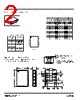
️· PCB Layout: The document includes a diagram for the recommended PCB layout.
️· Patents: The device incorporates technology covered by U.S. patents.
If you have any other questions about specific aspects of the OP4017B, feel free to ask!
1. General Description:
️· Type: Voltage-Controlled Crystal Oscillator (VCXO) / Voltage-Controlled Oscillator (VCO). Essentially a precise clock generator.
️· Frequency: 77.112 MHz
️· Purpose: Designed for optical communication systems (like fiber optics) and other applications requiring a stable, precise clock.
️· CAUTION: Electrostatic Sensitive Device - requires careful handling.
️· Export Restriction: Requires approval from the U.S. Department of Commerce for export.
2. Key Specifications:
️· Operating Voltage: 3.3V or 5.0V (nominal)
️· Frequency Stability: (Specific figures are complex and dependent on conditions; see the full datasheet)
️· Jitter: Very low jitter is a critical feature for optical applications. The datasheet provides detailed figures.
️· Phase Noise: Extremely low phase noise, a crucial characteristic.
️· Dimensions: See the table of dimensions (approx. 13.46 x 9.14mm)
3. Electrical Connections:
️· Pin 1: VCC (Power Supply)
️· Pin 2: Ground
️· Pin 3: Enable/Disable (Controls whether the oscillator is active)
️· Pin 4 & 5: Q Output (Clock signal output)
️· Pin 6: Ground
️· Pin 8: Tuning Input (Voltage used to adjust the output frequency)
️· LID: Ground
4. Important Notes:
️· Datasheet Dependency: Many critical performance characteristics (stability, jitter, phase noise) are complex and fully detailed in the complete datasheet. The summary provided gives general information.
️· PCB Layout: The document includes a diagram for the recommended PCB layout.
️· Patents: The device incorporates technology covered by U.S. patents.
| Part No. | OP4017B1 |
| Manufacturer | MURATA |
| Size | 71 Kbytes |
| Pages | 2 pages |
| Description | 777.60 MHz Optical Timing Clock |
| Does ALLDATASHEET help your business so far? [ DONATE ] |
About Alldatasheet | Advertisement | Contact us | Privacy Policy | Link to Datasheet | Link Exchange | Manufacturer List All Rights Reserved©Alldatasheet.com |
| Russian : Alldatasheetru.com | Korean : Alldatasheet.co.kr | Spanish : Alldatasheet.es | French : Alldatasheet.fr | Italian : Alldatasheetit.com Portuguese : Alldatasheetpt.com | Polish : Alldatasheet.pl | Vietnamese : Alldatasheet.vn Indian : Alldatasheet.in | Mexican : Alldatasheet.com.mx | British : Alldatasheet.co.uk | New Zealand : Alldatasheet.co.nz |
|
Family Site : ic2ic.com |
icmetro.com |
 British ▼
  English
 Chinese
 German
 Japanese
 Russian
 Korean
 Spanish
 French
 Italian
 Portuguese
 Polish
 Vietnamese
 Indian
 Mexican
 New Zealand