|
Electronic Components Datasheet Search |
|
|
Electronic Components Datasheet Search |
|
M54617P Datasheet(PDF) 2 Page - Mitsubishi Electric Semiconductor |
|
|
|||||||||||||||||||||||||||||
M54617P Datasheet(HTML) 2 Page - Mitsubishi Electric Semiconductor |
|
|
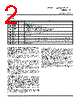
2 / 8 page  LAN TRANSCEIVER M54617P MITSUBISHI <CONTROL / DRIVER IC> FUNCTION Pin function Pin No. Pin name I/O Function TX Input Data signal input pin STB Input Standby signal input pin L: standby mode, H: normal operation ERR I/O Error signal output pin and error reset input pin “L” level output when abnormal transmission route is detected Error reset with “H” level input when in the standby mode RX Output Signal output pin from transmission route VSS Input Grounding pin BUS(-) I/O Signal output pin to transmission route and signal input pin from transmission route (negative logic) BUS(+) I/O Signal output pin to transmission route and signal input pin from transmission route (positive logic) Power supply pin VDD Input 1 2 3 4 5 6 7 8 ABNORMALITY DETECTION OF TRANSMISSION ROUTE AND COMMUNICATION FUNCTION The M54617P uses its driver overcurrent detection function and transmission signal logic abnormality function to perform the abnormality detection of the transmission route, and outputs error signal (ERR(3 pin) = “L”). In addition, switching the signal that is output to Rx pin (pin 4) according to the abnormality occurrence status permits communication after abnormality has occurred. (1) Overcurrent detection BUS(+) pin (pin 7) and BUS(-) pin (pin 6) drivers of M54617P are equipped with an overcurrent detection circuit. When overcurrent flows to a driver, the driver is turned OFF to output error signal (ERR (pin 3) = “L”). Once an overcurrent is detected, the driver maintains the OFF status until the error is reset. In addition, each driver of BUS(+) pin (pin 7) and BUS(-) pin (pin 6) is independent, and both may be turned OFF depending upon the abnormality occurrence status. A built-in filter for the prevention of malfunction due to overcurrent when the driver is turned ON does not permit the detection of the overcurrent status for a short time (several hundred ns). Detection current is set to about 180mA. (2) Logic abnormality detection The M54617P transmission signals operate in the opposite phase to each other, and abnormal transmission route is detected by comparing these signals. Upon comparing respective signals after a set time on the basis of the edge of transmission routes BUS(+) and BUS(-), any disagreement is regarded as abnormal transmission, and error signal (ERR (pin 3) = “L”) is output. In order to be well timed with that edge as a new standard, abnormality is detected when signal disagreement continues for more than a set time. Setting time is set to about 4.2 µs. Logic abnormality detection does not cope with more than one error mode. Detection of logic abnormality alone does not allow the driver to be turned OFF. Abnormality detection allows the driver to be turned OFF only when overcurrent is detected. (3) Communication function The M54617P ordinarily outputs the differential signals of BUS(+) (pin 7) and BUS(-) (pin 6). When abnormality is detected, signals to be output to Rx pin (pin 4) are switched according to the status. When overcurrent is detected, the driver or the transmission route in which overcurrent is detected is considered abnormal, and error signal is output, and concurrently the signal of another transmission route is output to Rx output (pin 4). As described in the above section (1), both drivers are turned OFF in some cases. In these cases, Rx output (pin 4) is fixed to “L”. When logic abnormality is detected, error signal (ERR (pin 3) = “L”) is output, and concurrently Rx output (pin 4) is turned to “L”. After error signal is output, the transmission route in which the edge of transmission signals is detected is considered normal, and such signal is output to Rx output (pin 4). In switching operation of error signal output and Rx output the priority is given to overcurrent detection over logic abnormality detection. |
|
|
Link URL |
| Does ALLDATASHEET help your business so far? [ DONATE ] |
About Alldatasheet | Advertisement | Contact us | Privacy Policy | Link to Datasheet | Link Exchange | Manufacturer List All Rights Reserved©Alldatasheet.com |
| Russian : Alldatasheetru.com | Korean : Alldatasheet.co.kr | Spanish : Alldatasheet.es | French : Alldatasheet.fr | Italian : Alldatasheetit.com Portuguese : Alldatasheetpt.com | Polish : Alldatasheet.pl | Vietnamese : Alldatasheet.vn Indian : Alldatasheet.in | Mexican : Alldatasheet.com.mx | British : Alldatasheet.co.uk | New Zealand : Alldatasheet.co.nz |
|
Family Site : ic2ic.com |
icmetro.com |
 British ▼
 English
 Chinese
 German
 Japanese
 Russian
 Korean
 Spanish
 French
 Italian
 Portuguese
 Polish
 Vietnamese
 Indian
 Mexican
 British
 New Zealand