|
Electronic Components Datasheet Search |
|
|
Electronic Components Datasheet Search |
|
M8880 Datasheet(PDF) 3 Page - Clare, Inc. |
|
|
|||||||||||||||||||||||||||||
M8880 Datasheet(HTML) 3 Page - Clare, Inc. |
|
|
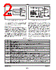
3 / 13 page  causes VC (see Figure 5) to rise as the capacitor discharges. Provided that the signal condition is maintained (ESt remains high) for the validation period (tGTP), VC reaches the threshold (VTSt) of the steering logic to register the tone pair, latching its corresponding 4-bit code (see Table 2) into the receive data reg- ister. At this point the StGT output is activated and drives VC to VDD. StGT continues to drive high as long as ESt remains high. Finally, after a short delay to allow the output latch to settle, the delayed steering output flag goes high, signaling that a received tone pair has been registered. It is possible to monitor the status of the delayed steering flag by checking the appropriate bit in the status register. If interrupt mode has been selected, the IRQ/CP pin will pull low when the delayed steering flag is active. The contents of the output latch are updated on an active de- layed steering transition. This data is presented to the 4-bit bidirectional data bus when the receive data register is read. The steering circuit works in reverse to validate the interdigit pause between signals. Thus, as well as rejecting signals too short to be considered valid, the receiver will tolerate signal in- terruptions (dropout) too short to be considered a valid pause. This capability, together with the ability to select the steering time constants externally, allows the designer to tailor perfor- mance to meet a wide variety of system requirements. Guard Time Adjustment: The simple steering circuit shown in Figure 5 is adequate for most applications. Component values are chosen according to the formula: tREC =tDP +tGTP TID =tDA +tGTA The value of tDP is a device parameter and tREC is the minimum signal duration to be recognized by the receiver. A value for C1 of 0.1 µF is recommended for most applications, leaving R1 to be selected by the designer. Different steering arrangements may be used to select independently the guard times for tone present (tGTP) and tone absent (tGTA). This may be necessary to meet system specifications that place both accept and reject limits on both tone duration and interdigit pause. Guard time ad- justment also allows the designer to tailor system parameters such as talkoff and noise immunity. Increasing tREC improves talkoff performance since it reduces the probability that tones simulated by speech will maintain signal condition long enough to be registered. Alternatively, a relatively short tREC with a long tDO would be appropriate for extremely noisy environments where fast acquisition time and immunity to tone dropouts are required. Design information for guard time adjustment is shown in Figure 6. Call Progress Filter A call progress (CP) mode can be selected, allowing the detec- tion of various tones that identify the progress of a telephone call on the network. The call progress tone input and DTMF input are common; however, call progress tones can only be detected when the CP mode has been selected. DTMF signals cannot be Page 3 M-8880 40-406-00012, Rev. G www.clare.com FLOW FHIGH Digit D3 D2 D1 D0 697 1209 10001 697 1336 20010 697 1477 30011 770 1209 40100 770 1336 50101 770 1477 60110 852 1209 70111 852 1336 81000 852 1477 91001 941 1336 01010 941 1209 * 1011 941 1477 #1100 697 1633 A 1101 770 1633 B 1110 852 1633 C 1111 941 1633 D 0000 0 = logic low, 1 = logic high Table 2 Tone Encoding/Decoding Figure 5 Basic Steering Circuit Figure 6 Guard Time Adjustment |
|
|
Link URL |
| Does ALLDATASHEET help your business so far? [ DONATE ] |
About Alldatasheet | Advertisement | Contact us | Privacy Policy | Link to Datasheet | Link Exchange | Manufacturer List All Rights Reserved©Alldatasheet.com |
| Russian : Alldatasheetru.com | Korean : Alldatasheet.co.kr | Spanish : Alldatasheet.es | French : Alldatasheet.fr | Italian : Alldatasheetit.com Portuguese : Alldatasheetpt.com | Polish : Alldatasheet.pl | Vietnamese : Alldatasheet.vn Indian : Alldatasheet.in | Mexican : Alldatasheet.com.mx | British : Alldatasheet.co.uk | New Zealand : Alldatasheet.co.nz |
|
Family Site : ic2ic.com |
icmetro.com |
 British ▼
 English
 Chinese
 German
 Japanese
 Russian
 Korean
 Spanish
 French
 Italian
 Portuguese
 Polish
 Vietnamese
 Indian
 Mexican
 British
 New Zealand