|
Electronic Components Datasheet Search |
|
|
Electronic Components Datasheet Search |
|
MSM6242B Datasheet(PDF) 10 Page - OKI electronic componets |
|
|
|||||||||||||||||||||||||||||
MSM6242B Datasheet(HTML) 10 Page - OKI electronic componets |
|
|
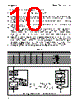
10 / 18 page  ¡ Semiconductor MSM6242B 32 FUNCTIONAL DESCRIPTION OF REGISTERS S 1, S10, MI1, MI10, H1, H10, D1, D10, MO1, MO10, Y1, Y10, W a) These are abbreviations for SECOND1, SECOND10, MINUTE1, MINUTE10, HOUR1, HOUR10, DAY1, DAY10, MONTH1, MONTH10, YEAR1, YEAR10, and WEEK. These values are in BCD notation. b) All registers are logically positive. For example, (S8, S4, S2, S1) = 1001 which means 9 seconds. c) If data is written which is out of the clock register data limits, it can result in erroneous clock data being read back. d) PM/AM, h 20, h10 In the mode setting of 24-hour mode, PM/AM bit is ignored, while in the setting of 12-hour mode h 20 is to be set. Otherwise it causes a discrepancy. In reading out the PM/AM bit in the 24-hour mode, it is continuously read out as 0. In reading out h 20 bit in the 12-hour mode, 0 is written into this bit first, then it is continuously read out as 0 unless 1 is being written into this bit. e) Registers Y1, Y10, and Leap Year. The MSM6242B is designed exclusively for the Christian Era and is capable of identifying a leap year automatically. The result of the setting of a non- existant day of the month is shown in the following example: If the date February 29 or November 31, 1985, was written, it would be changed automatically to March 1, or December 1, 1985 at the exact time at which a carry pulse occurs for the day's digit. f) The Register W data limits are 0 – 6 (Tabel 1 shows a possible data definition). TABLE 1 w4 0 0 0 0 1 1 1 w2 0 0 1 1 0 0 1 w1 0 1 0 1 0 1 0 Day of Week Sunday Monday Tuesday Wednesday Thursday Friday Saturday HOLD Bit ← 1 Write data into or Read data from registers S1 ~ W Busy Bit= O? Read BUSY Bit Read Register S1 ~ W Data of S1 ~ W Register DATA ← DATA1 = DATA2 YES NO First Second Using HOLD Bit Not Using HOLD Bit HOLD Bit ← 0 Figure 10. Reading and Writing of Registers S1 ~ W Read Register S1 ~ W DATA1 = DATA2 YES NO * In the inside of LSI, the CLEAR of BUSY bit is performed when HOLD bit = 0, but, if the period of HOLD bit =0 is extermely narrow as compared with the period of HOLD bit = 1, there is some case that the CLEAR of BUSY bit delays so that the BUSY bit can be cleared by sampling HOLD bit = 0 at approximate 16KHz. It is recommended to allow an idling time of 62ms or more. * Idling Time HOLD Bit ← 0 |
|
|
Link URL |
| Does ALLDATASHEET help your business so far? [ DONATE ] |
About Alldatasheet | Advertisement | Contact us | Privacy Policy | Link to Datasheet | Link Exchange | Manufacturer List All Rights Reserved©Alldatasheet.com |
| Russian : Alldatasheetru.com | Korean : Alldatasheet.co.kr | Spanish : Alldatasheet.es | French : Alldatasheet.fr | Italian : Alldatasheetit.com Portuguese : Alldatasheetpt.com | Polish : Alldatasheet.pl | Vietnamese : Alldatasheet.vn Indian : Alldatasheet.in | Mexican : Alldatasheet.com.mx | British : Alldatasheet.co.uk | New Zealand : Alldatasheet.co.nz |
|
Family Site : ic2ic.com |
icmetro.com |
 British ▼
 English
 Chinese
 German
 Japanese
 Russian
 Korean
 Spanish
 French
 Italian
 Portuguese
 Polish
 Vietnamese
 Indian
 Mexican
 British
 New Zealand