|
Electronic Components Datasheet Search |
|
|
Electronic Components Datasheet Search |
|
INMP401ACEZ-R0 Datasheet(PDF) 8 Page - TDK Electronics |
|
|
|||||||||||||||||||||||||||||
INMP401ACEZ-R0 Datasheet(HTML) 8 Page - TDK Electronics |
|
|
8 / 14 page 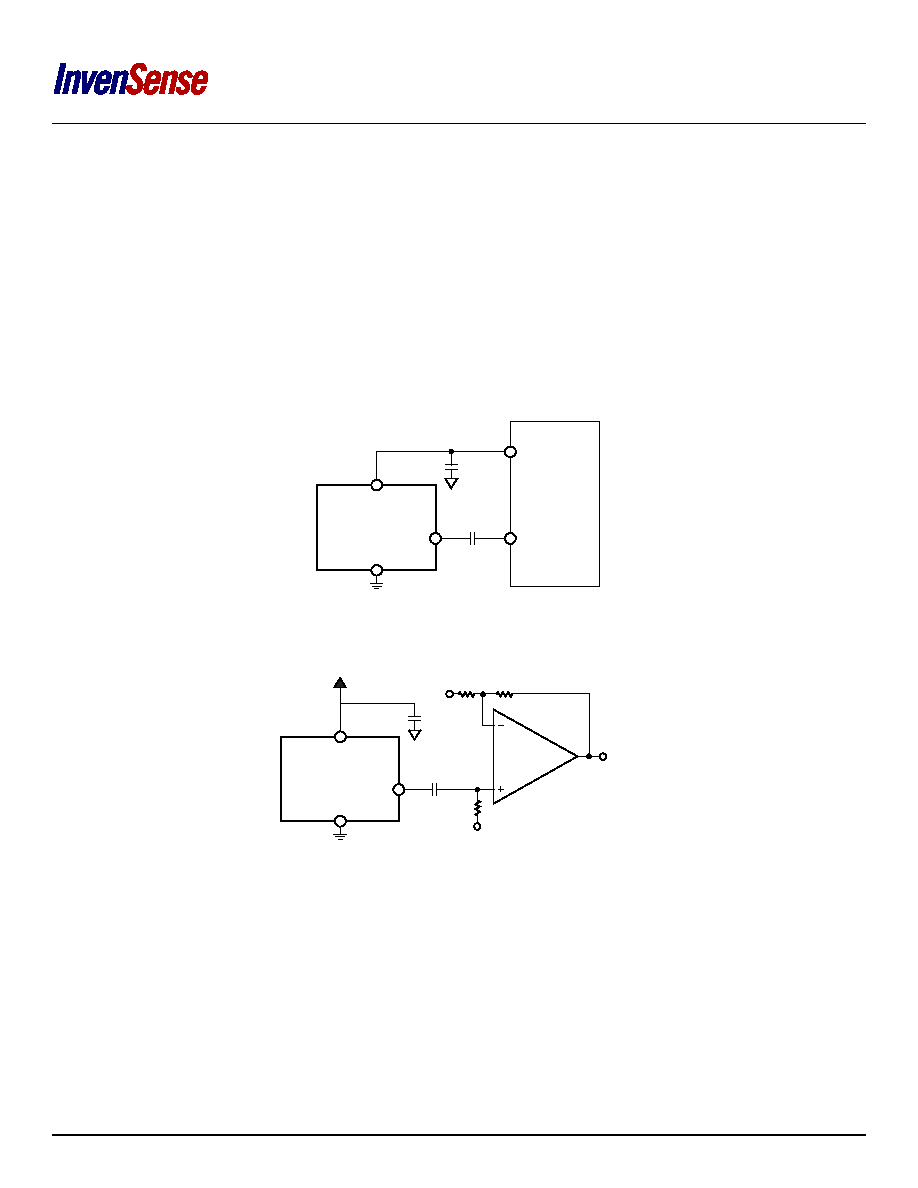 INMP401 APPLICATIONS INFORMATION CONNECTING TO AUDIO CODECS The INMP401 output can be connected to a dedicated codec microphone input (see Figure 6) or to a high input impedance gain stage (see Figure 7.) A 0.1 µF ceramic capacitor placed close to the INMP401 supply pin is used for testing and is recommended to adequately decouple the microphone from noise on the power supply. A DC-blocking capacitor is required at the output of the microphone. This capacitor creates a high-pass filter with a corner frequency at fC = 1/(2π × C × R) where R is the input impedance of the codec. A minimum value of 2.2 µF is recommended in Figure 6 because the input impedance of codecs can be as low as 2 kΩ at its highest PGA gain setting, which results in a high-pass filter corner frequency at about 37 Hz. Figure 7 shows the INMP401 connected to an op amp configured as a non-inverting preamplifier. Figure 6. INMP401 Connected to a Codec Figure 7. INMP401 Connected to an Op Amp ADC OR CODEC INMP401 GND OUTPUT INPUT MICBIAS 2.2 µF MINIMUM 0.1 µF VDD GAIN = (R1 + R2)/R1 INMP401 GND OUTPUT 1µF MINIMUM 0.1µF 10k Ω R1 R2 VDD VREF VOUT VREF AMP 1.8-3.3 V Page 8 of 14 Document Number: DS-INMP401-00 Revision: 1.0. |
|
|
Link URL |
| Does ALLDATASHEET help your business so far? [ DONATE ] |
About Alldatasheet | Advertisement | Contact us | Privacy Policy | Link to Datasheet | Link Exchange | Manufacturer List All Rights Reserved©Alldatasheet.com |
| Russian : Alldatasheetru.com | Korean : Alldatasheet.co.kr | Spanish : Alldatasheet.es | French : Alldatasheet.fr | Italian : Alldatasheetit.com Portuguese : Alldatasheetpt.com | Polish : Alldatasheet.pl | Vietnamese : Alldatasheet.vn Indian : Alldatasheet.in | Mexican : Alldatasheet.com.mx | British : Alldatasheet.co.uk | New Zealand : Alldatasheet.co.nz |
|
Family Site : ic2ic.com |
icmetro.com |
 British ▼
 English
 Chinese
 German
 Japanese
 Russian
 Korean
 Spanish
 French
 Italian
 Portuguese
 Polish
 Vietnamese
 Indian
 Mexican
 British
 New Zealand