 |
Electronic Components Datasheet Search |
|
|
Electronic Components Datasheet Search |
|
PCF8564A Datasheet(PDF) 44 Page - NXP Semiconductors |
|
|
|||||||||||||||||||||||||||||
PCF8564A Datasheet(HTML) 44 Page - NXP Semiconductors |
|
|
44 / 59 page 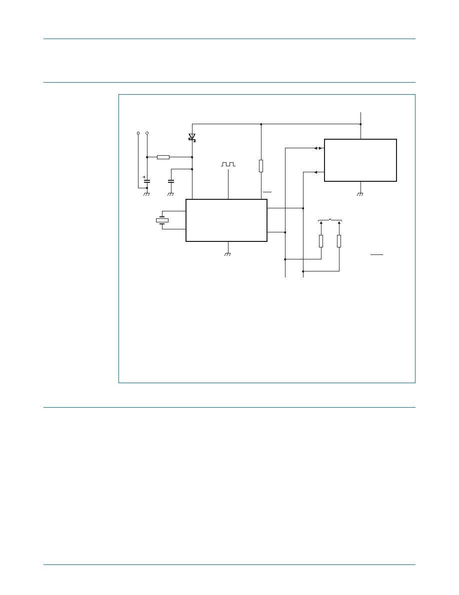 PCA85063A All information provided in this document is subject to legal disclaimers. © NXP Semiconductors N.V. 2018. All rights reserved. Product data sheet Rev. 4 — 30 March 2018 44 of 59 NXP Semiconductors PCA85063A Automotive Real-Time Clock/calendar with alarm function and I2C-bus 14. Application information 15. Test information 15.1 Quality information This product has been qualified in accordance with the Automotive Electronics Council (AEC) standard Q100 - Failure mechanism based stress test qualification for integrated circuits, and is suitable for use in automotive applications. A 1 farad super capacitor combined with a low VF diode can be used as a standby or back-up supply. With the RTC in its minimum power configuration that is, timer off and CLKOUT off, the RTC may operate for weeks. (1) R1 limits the inrush current to the super capacitor at power-on. (2) NXP recommends tying VDD of the device and VDD of all the external pull-up resistors to the same Power Supply. (3) NXP also recommends the customer place accessible 'Pads/TP-test point' on the layout so as to enable a 'hard'' grounding of the power supply VDD in the event a full discharge cannot be attained. Fig 29. Application diagram for PCA85063A PCA85063A MASTER TRANSMITTER/ RECEIVER OSCI OSCO VSS SDA R aaa-013719 R SCL SDA (I2C-bus) SCL SDA SCL INT VDD VDD(2) VDD(2) 1 F R1(1) TP(3) 100 nF R: pull-up resistor R = tr Cb CLKOUT |
|
Link URL |
| Does ALLDATASHEET help your business so far? [ DONATE ] |
About Alldatasheet | Advertisement | Contact us | Privacy Policy | Link to Datasheet | Link Exchange | Manufacturer List All Rights Reserved©Alldatasheet.com |
| Russian : Alldatasheetru.com | Korean : Alldatasheet.co.kr | Spanish : Alldatasheet.es | French : Alldatasheet.fr | Italian : Alldatasheetit.com Portuguese : Alldatasheetpt.com | Polish : Alldatasheet.pl | Vietnamese : Alldatasheet.vn Indian : Alldatasheet.in | Mexican : Alldatasheet.com.mx | British : Alldatasheet.co.uk | New Zealand : Alldatasheet.co.nz |
|
Family Site : ic2ic.com |
icmetro.com |
 British ▼
 English
 Chinese
 German
 Japanese
 Russian
 Korean
 Spanish
 French
 Italian
 Portuguese
 Polish
 Vietnamese
 Indian
 Mexican
 British
 New Zealand


