 |
Electronic Components Datasheet Search |
|
|
Electronic Components Datasheet Search |
|
XIO2000 Datasheet(PDF) 32 Page - Texas Instruments |
|
|
|||||||||||||||||||||||||||||
XIO2000 Datasheet(HTML) 32 Page - Texas Instruments |
|
|
32 / 150 page 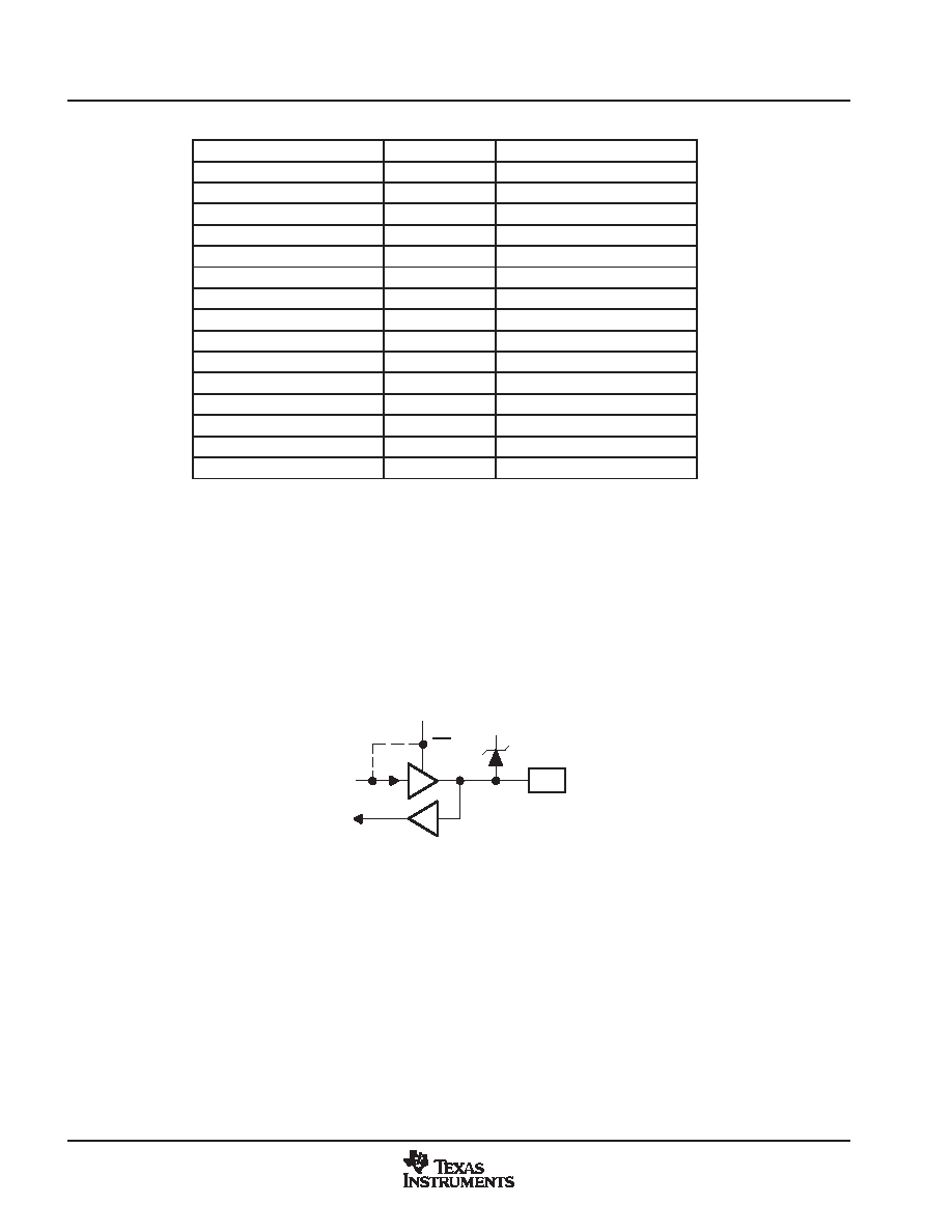 Feature/Protocol Descriptions 20 November 2005 SCPS097B Table 3−3. Messages Supported by the Bridge MESSAGE SUPPORTED BRIDGE ACTION Assert_INTx Yes Transmitted upstream Deassert_INTx Yes Transmitted upstream PM_Active_State_Nak Yes Received and processed PM_PME Yes Transmitted upstream PME_Turn_Off Yes Received and processed PME_TO_Ack Yes Transmitted upstream ERR_COR Yes Transmitted upstream ERR_NONFATAL Yes Transmitted upstream ERR_FATAL Yes Transmitted upstream Unlock Yes Received and processed Set_Slot_Power_Limit Yes Received and processed Hot plug messages No Discarded Advanced switching messages No Discarded Vendor defined type 0 No Unsupported request Vendor defined type 1 No Discarded All supported message transactions are processed per the PCI Express Base Specification. 3.4 PCI Bus Interface 3.4.1 I/O Characteristics Figure 3−4 shows a 3-state bidirectional buffer that represents the I/O cell design for the PCI bus. Section 7.6, Electrical Characteristics over Recommended Operating Conditions, provides the electrical characteristics of the PCI bus I/O cell. NOTE: The PCI bus interface on the bridge meets the ac specifications of the PCI Local Bus Specification. Additionally, PCI bus terminals (input or I/O) must be held high or low to prevent them from floating. Tied for Open Drain OE Pad VCCP Figure 3−4. 3-State Bidirectional Buffer 3.4.2 Clamping Voltage In the bridge, the PCI bus I/O drivers are powered from the VDD_33 power rail. Plus, the I/O driver cell is tolerant to input signals with 5.0-V peak-to-peak amplitudes. For PCI bus interfaces operating at 66 MHz, all devices are required to output only 3.3-V peak-to-peak signal amplitudes. For PCI bus interfaces operating at 33 MHz, devices may output either 3.3-V or 5.0-V peak-to-peak signal amplitudes. The bridge accommodates both signal amplitudes. Each PCI bus I/O driver cell has a clamping diode connected to the VCCP voltage rail that protects the cell from excessive input voltage. If the PCI signaling is 3.3 V, then VCCP (A04, J01) is connected to a 3.3-V power supply. If the PCI signaling is 5.0 V, then VCCP (A04, J01) is connected to a 5.0-V power supply. |
|
Link URL |
| Does ALLDATASHEET help your business so far? [ DONATE ] |
About Alldatasheet | Advertisement | Contact us | Privacy Policy | Link to Datasheet | Link Exchange | Manufacturer List All Rights Reserved©Alldatasheet.com |
| Russian : Alldatasheetru.com | Korean : Alldatasheet.co.kr | Spanish : Alldatasheet.es | French : Alldatasheet.fr | Italian : Alldatasheetit.com Portuguese : Alldatasheetpt.com | Polish : Alldatasheet.pl | Vietnamese : Alldatasheet.vn Indian : Alldatasheet.in | Mexican : Alldatasheet.com.mx | British : Alldatasheet.co.uk | New Zealand : Alldatasheet.co.nz |
|
Family Site : ic2ic.com |
icmetro.com |
 British ▼
 English
 Chinese
 German
 Japanese
 Russian
 Korean
 Spanish
 French
 Italian
 Portuguese
 Polish
 Vietnamese
 Indian
 Mexican
 British
 New Zealand


