|
Electronic Components Datasheet Search |
|
|
Electronic Components Datasheet Search |
|
LT3960 Datasheet(PDF) 8 Page - Analog Devices |
|
|
|||||||||||||||||||||||||||||
LT3960 Datasheet(HTML) 8 Page - Analog Devices |
|
|
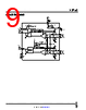
8 / 22 page  LT3960 8 Rev. B For more information www.analog.com PIN FUNCTIONS CANSDAL (Pin 1): Low Level CAN Bus Line. Carries the I2C data bus. CANSDAH (Pin 2): High Level CAN Bus Line. Carries the I2C data bus. CANSCLH (Pin 4): High Level CAN Bus Line. Carries the I2C clock bus. CANSCLL (Pin 5): Low Level CAN Bus Line. Carries the I2C clock bus. GND (Pin 3 and Exposed Pad): Ground. Solder the exposed pad and pin directly to the ground plane. VIN (Pin 6): Input Voltage Supply. This pin is the power supply input to the LDO. It must be locally bypassed with a 1µF filter capacitor to GND as close to the pin as possi- ble. If the LDO function is unused, tie VIN to VCC. EN/MODE (Pin 7): MODE/Shutdown pin. Tie above 2.5V to select master mode, float pin to select slave mode, or pull this pin to ground for low-power shutdown mode. VCC (Pin 8): Low Dropout Regulator Output and Device Power Supply Input. Bypass this pin with a 2.2µF or greater capacitor to ground. Any bypass capacitors must be located as close to the pin as possible. SCL (Pin 9): Clock Input or Output Pin for the I2C Serial Port. When EN/MODE is 2.5V or above, the SCL pin is an input for the master clock. When EN/MODE is float- ing, the SCL pin is an output for data received on the CANSCLH/L pins. SDA (Pin 10): Data Input and Output Pin for the I2C Serial Port. |
|
|
Link URL |
| Does ALLDATASHEET help your business so far? [ DONATE ] |
About Alldatasheet | Advertisement | Contact us | Privacy Policy | Link to Datasheet | Link Exchange | Manufacturer List All Rights Reserved©Alldatasheet.com |
| Russian : Alldatasheetru.com | Korean : Alldatasheet.co.kr | Spanish : Alldatasheet.es | French : Alldatasheet.fr | Italian : Alldatasheetit.com Portuguese : Alldatasheetpt.com | Polish : Alldatasheet.pl | Vietnamese : Alldatasheet.vn Indian : Alldatasheet.in | Mexican : Alldatasheet.com.mx | British : Alldatasheet.co.uk | New Zealand : Alldatasheet.co.nz |
|
Family Site : ic2ic.com |
icmetro.com |
 British ▼
 English
 Chinese
 German
 Japanese
 Russian
 Korean
 Spanish
 French
 Italian
 Portuguese
 Polish
 Vietnamese
 Indian
 Mexican
 British
 New Zealand