 |
Electronic Components Datasheet Search |
|
|
Electronic Components Datasheet Search |
|
PCF8563 Datasheet(PDF) 21 Page - NXP Semiconductors |
|
|
|||||||||||||||||||||||||||||
PCF8563 Datasheet(HTML) 21 Page - NXP Semiconductors |
|
|
21 / 30 page 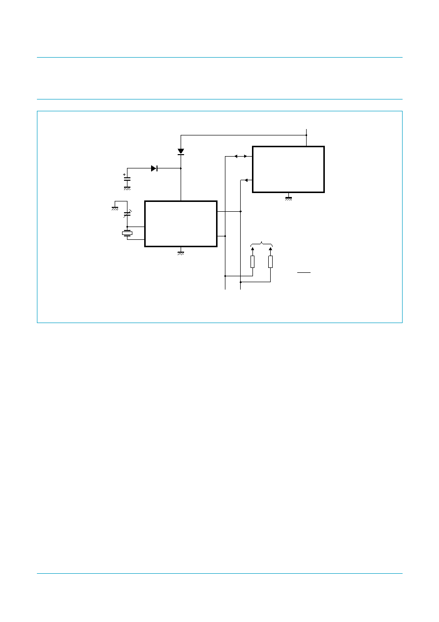 Philips Semiconductors PCF8563 Real-time clock/calendar Product specification 16 April 1999 21 of 30 9397 750 04855 © Philips Electronics N.V. 1999. All rights reserved. 12. Application information 12.1 Quartz crystal frequency adjustment Method 1: Fixed OSCI capacitor — By evaluating the average capacitance necessary for the application layout a fixed capacitor can be used. The frequency is best measured via the 32.768 kHz signal available after power-on at the CLKOUT pin. The frequency tolerance depends on the quartz crystal tolerance, the capacitor tolerance and the device-to-device tolerance (on average ±5 × 10⁻⁶). Average deviations of ±5 minutes per year can be easily achieved. Method 2: OSCI trimmer — The oscillator is tuned to the required accuracy by adjusting a trimmer capacitor on pin OSCI and measuring the 32.768 kHz signal available after power-on at the CLKOUT pin. Method 3: OSCO output — Direct output measurement on pin OSCO (accounting for test probe capacitance). Fig 19. Application diagram. handbook, full pagewidth MGM665 SCL SDA VSS OSCI OSCO CLOCK CALENDAR PCF8563 SDA SCL MASTER TRANSMITTER/ RECEIVER VDD VDD SDA SCL RR VDD (I2C-bus) R: pull-up resistor R = 1 F tr Cb |
|
Link URL |
| Does ALLDATASHEET help your business so far? [ DONATE ] |
About Alldatasheet | Advertisement | Contact us | Privacy Policy | Link to Datasheet | Link Exchange | Manufacturer List All Rights Reserved©Alldatasheet.com |
| Russian : Alldatasheetru.com | Korean : Alldatasheet.co.kr | Spanish : Alldatasheet.es | French : Alldatasheet.fr | Italian : Alldatasheetit.com Portuguese : Alldatasheetpt.com | Polish : Alldatasheet.pl | Vietnamese : Alldatasheet.vn Indian : Alldatasheet.in | Mexican : Alldatasheet.com.mx | British : Alldatasheet.co.uk | New Zealand : Alldatasheet.co.nz |
|
Family Site : ic2ic.com |
icmetro.com |
 British ▼
 English
 Chinese
 German
 Japanese
 Russian
 Korean
 Spanish
 French
 Italian
 Portuguese
 Polish
 Vietnamese
 Indian
 Mexican
 British
 New Zealand


