|
Electronic Components Datasheet Search |
|
|
Electronic Components Datasheet Search |
|
S71PL129JC0 Datasheet(PDF) 21 Page - SPANSION |
|
|
|||||||||||||||||||||||||||||
S71PL129JC0 Datasheet(HTML) 21 Page - SPANSION |
|
|
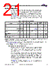
21 / 153 page  October 28, 2005 S71PL129Jxx_00_A8 S71PL129JC0/S71PL129JB0/S71PL129JA0 19 Advance Informatio n Device Bus Operations This section describes the requirements and use of the device bus operations, which are initiated through the internal command register. The command register itself does not occupy any addressable memory location. The register is a latch used to store the commands, along with the address and data information needed to execute the command. The contents of the register serve as inputs to the internal state machine. The state machine outputs dictate the function of the device. Table 1 lists the device bus operations, the inputs and control levels re- quired, and the resulting output. The following subsections describe each of these operations in further detail. Legend: L = Logic Low = VIL, H = Logic High = VIH, VID = 11.5–12.5 V, VHH = 8.5–9.5 V, X = Don’t Care, SA = Sector Address, AIN = Address In, DIN = Data In, DOUT = Data Out Notes: 1. The sector protect and sector unprotect functions may also be implemented via programming equipment. See ““High Voltage Sector Protection” on page 37.” 2. WP#/ACC must be high when writing to upper two and lower two sectors. Requirements for Reading Array Data To read array data from the outputs, the system must drive the OE# and appro- priate CE# pins to VIL. In PL129J, CE1# and CE2# are the power control and select the lower (CE1#) or upper (CE2#) halves of the device. CE# is the power control. OE# is the output control and gates array data to the output pins. WE# should remain at VIH. The internal state machine is set for reading array data upon device power-up, or after a hardware reset. This ensures that no spurious alteration of the memory content occurs during the power transition. No command is necessary in this mode to obtain array data. Standard microprocessor read cycles that assert valid addresses on the device address inputs produce valid data on the device data outputs. Each bank remains enabled for read access until the command register contents are altered. See Table 24 for timing specifications and Figure 11 for the timing diagram. ICC1 in the DC Characteristics table represents the active current specification for reading array data. Table 1. PL129J Device Bus Operations Operation CE1# CE2# OE# WE# RESET# WP#/ACC Addresses (A21–A0) DQ15– DQ0 Read L H L H H X AIN DOUT H L Write L H H L H X (Note 2) AIN DIN H L Standby VIO± 0.3 V VIO ± 0.3 V X X VIO ± 0.3 V X X High-Z Output Disable L L H H H X X High-Z Reset X X X X L X X High-Z Temporary Sector Unprotect (High Voltage) X X X X VID X AIN DIN |
|
Link URL |
| Does ALLDATASHEET help your business so far? [ DONATE ] |
About Alldatasheet | Advertisement | Contact us | Privacy Policy | Link to Datasheet | Link Exchange | Manufacturer List All Rights Reserved©Alldatasheet.com |
| Russian : Alldatasheetru.com | Korean : Alldatasheet.co.kr | Spanish : Alldatasheet.es | French : Alldatasheet.fr | Italian : Alldatasheetit.com Portuguese : Alldatasheetpt.com | Polish : Alldatasheet.pl | Vietnamese : Alldatasheet.vn Indian : Alldatasheet.in | Mexican : Alldatasheet.com.mx | British : Alldatasheet.co.uk | New Zealand : Alldatasheet.co.nz |
|
Family Site : ic2ic.com |
icmetro.com |
 British ▼
 English
 Chinese
 German
 Japanese
 Russian
 Korean
 Spanish
 French
 Italian
 Portuguese
 Polish
 Vietnamese
 Indian
 Mexican
 British
 New Zealand