 |
Electronic Components Datasheet Search |
|
|
Electronic Components Datasheet Search |
|
ADA4700-1ARDZ-R7 Datasheet(PDF) 21 Page - Analog Devices |
|
|
|||||||||||||||||||||||||||||
ADA4700-1ARDZ-R7 Datasheet(HTML) 21 Page - Analog Devices |
|
|
21 / 28 page 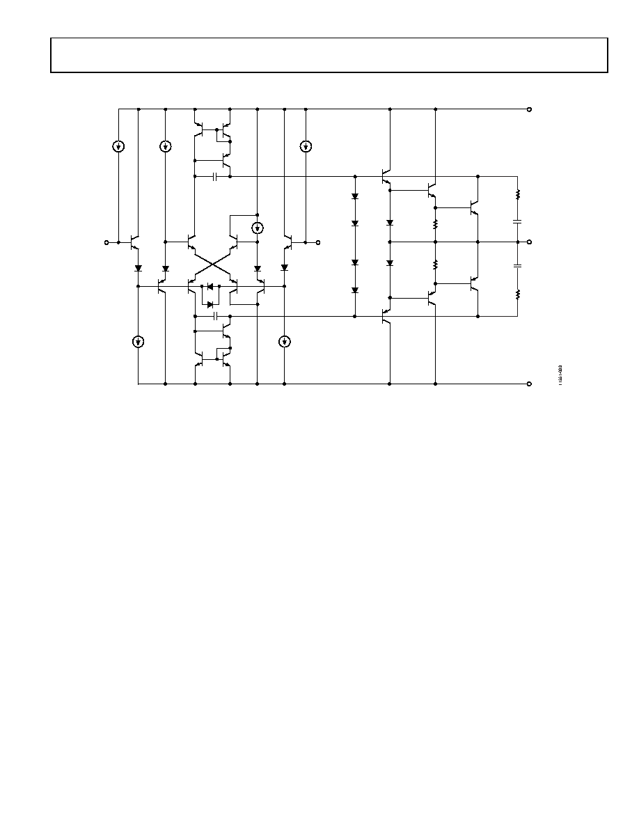 Data Sheet ADA4700-1 THEORY OF OPERATION Figure 58. Simplified Schematic of the ADA4700-1 The ADA4700-1 is a high voltage operational amplifier featuring a slew enhanced bipolar input stage that provides all of the voltage gain. Single stage amplifiers are noted for their excellent stability but poor open-loop gain; however, the advanced ADA4700-1 design provides gain comparable to multistage amplifiers and, therefore, combines the advantages of both. Referring to Figure 58, the input stage is formed by Q5 to Q8 loaded by the current mirrors, Q9 to Q14. The output stage is of the complementary Darlington type formed by Q15 to Q18. Like other bipolar amplifiers, the input stage is internally clamped to prevent degradation with large differential inputs; however, the addition of Q1 and Q2 in conjunction with the high voltage diodes, D1 and D2, maintain high differential input impedance even when the voltage between the inputs is equal to the supply voltage. This configuration makes the ADA4700-1 suitable for applications with unavoidable large differential voltages, such as rectifiers, peak detectors, and comparators. The ADA4700-1 uses a single-pole compensation set by C3 and C4. The internal snubber networks, R1/C1 and R2/C2, further enhance the stability. This design enables large capacitive loads to be driven without the risk of oscillation. The Q19 and Q20 transistors in conjunction with the R3 and R4 resistors provide output short-circuit protection. Additionally, a thermal regulating circuit (not shown in Figure 58) limits the die temperature to 145°C or greater to protect against excessive power dissipation. With approximately equal split supplies up to ±50 V, the output can be shorted to ground unconditionally; however, operating this way is not recommended. If the voltage between the output and either supply is more than 60 V, avoid a short circuit to the supply. Transient dissipation in the output transistors can exceed their safe operating area and cause subsequent destruction. THERMAL REGULATION The circuitry for thermal regulation of the ADA4700-1 is dependent on the ambient temperature and time duration of the current drive. When thermal regulation of the ADA4700-1 is active, the supply current, ISY, reduces from 1.7 mA to 300 µA. The output stage remains biased during thermal regulation due to the parasitics of the output devices in conjunction with the elevated die temperature. For example, with a current drive, IOUT, of 30 mA for 180 seconds and with an ambient temperature of 85°C, the thermal regulation is triggered at a junction temperature of 145°C with an output current level of 22 mA. For additional information, refer to the Thermal Management section and the Safe Operating Area section. R1 R3 10 Ω R4 10 Ω R2 C2 Q20 Q19 D9 D10 D6 D5 –IN I2 I1 I3 I4 D7 D2 D1 D3 D5 D6 C4 C3 D8 Q17 Q15 Q18 Q2 Q8 Q7 Q1 Q6 D4 Q4 Q5 Q10 +IN OUT V+ V– Q11 Q9 Q13 Q14 Q12 Q3 Q16 C1 I6 I5 Rev. 0 | Page 21 of 28 |
|
Link URL |
| Does ALLDATASHEET help your business so far? [ DONATE ] |
About Alldatasheet | Advertisement | Contact us | Privacy Policy | Link to Datasheet | Link Exchange | Manufacturer List All Rights Reserved©Alldatasheet.com |
| Russian : Alldatasheetru.com | Korean : Alldatasheet.co.kr | Spanish : Alldatasheet.es | French : Alldatasheet.fr | Italian : Alldatasheetit.com Portuguese : Alldatasheetpt.com | Polish : Alldatasheet.pl | Vietnamese : Alldatasheet.vn Indian : Alldatasheet.in | Mexican : Alldatasheet.com.mx | British : Alldatasheet.co.uk | New Zealand : Alldatasheet.co.nz |
|
Family Site : ic2ic.com |
icmetro.com |
 British ▼
 English
 Chinese
 German
 Japanese
 Russian
 Korean
 Spanish
 French
 Italian
 Portuguese
 Polish
 Vietnamese
 Indian
 Mexican
 British
 New Zealand


