 |
Electronic Components Datasheet Search |
|
|
Electronic Components Datasheet Search |
|
ADA4899-1YCPZ-R2 Datasheet(PDF) 13 Page - Analog Devices |
|
|
|||||||||||||||||||||||||||||
ADA4899-1YCPZ-R2 Datasheet(HTML) 13 Page - Analog Devices |
|
|
13 / 20 page 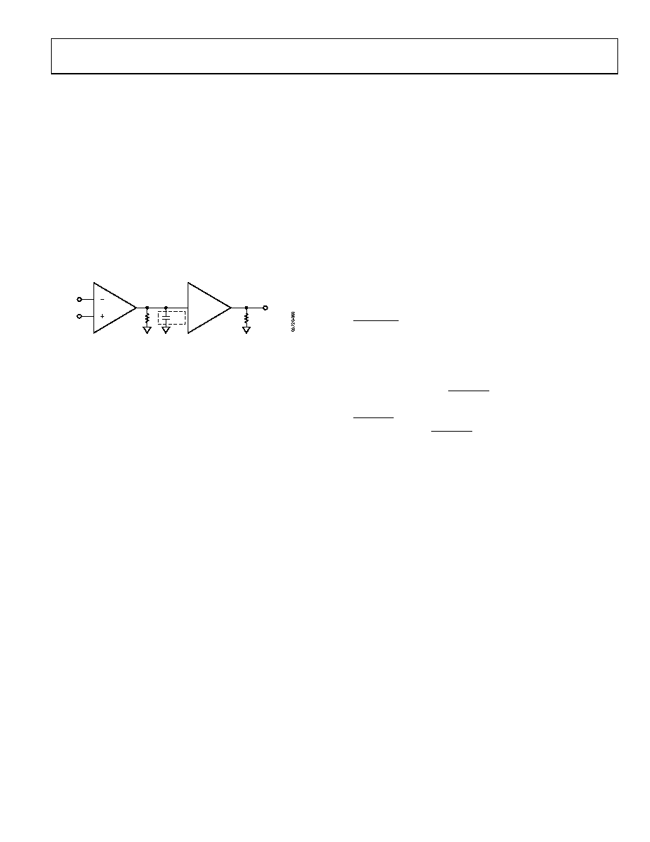 Data Sheet ADA4899-1 Rev. C | Page 13 of 20 THEORY OF OPERATION The ADA4899-1 is a voltage feedback op amp that combines unity-gain stability with a 1 nV/√Hz input noise. It employs a highly linear input stage that can maintain greater than −80 dBc (at 2 V p-p) distortion out to 10 MHz while in a unity-gain configuration. This rare combination of low gain stability, input-referred noise, and extremely low distortion is the result of Analog Devices proprietary op amp architecture and high speed complementary bipolar processing technology. The simplified ADA4899-1 topology, shown in Figure 45, is a single gain stage with a unity-gain output buffer. It has over 80 dB of open-loop gain and maintains precision specifications such as CMRR, PSRR, and offset to levels that are normally associated with topologies having two or more gain stages. BUFFER gm CC R1 RL VOUT Figure 45. ADA4899-1 Topology A pair of internally connected diodes limits the differential voltage between the noninverting input and the inverting input of the ADA4899-1. Each set of diodes has two series diodes connected in antiparallel, which limits the differential voltage between the inputs to approximately ±1.2 V. All of the ADA4899-1 pins are ESD protected with voltage-limiting diodes connected between both rails. The protection diodes can handle 10 mA. Currents should be limited through these diodes to 10 mA or less by using a series limiting resistor. PACKAGING INNOVATION The ADA4899-1 is available in both a SOIC and an LFCSP, each of which has a thermal pad that allows the device to run cooler, thereby increasing reliability. To help avoid routing around the pad when laying out the board, both packages have a dedicated feedback pin on the opposite side of the package for ease in connecting the feedback network to the inverting input. The secondary output pin also isolates the interaction of any capacitive load on the output and the self-inductance of the package and bond wire from the feedback loop. When using the dedicated feedback pin, inductance in the primary output helps to isolate capacitive loads from the output impedance of the amplifier. Both the SOIC and LFCSP have modified pinouts to improve heavy load second harmonic distortion performance. The intent of both is to isolate the negative supply pin from the noninverting input. The LFCSP accomplishes this by rotating the standard 8-lead package pinout counterclockwise by one pin, which puts the supply and output pins on the right side of the package and the input pins on the left side of the package. The SOIC is slightly different with the intent of both isolating the inputs from the supply pins and giving the user the option of using the ADA4899-1 in a standard SOIC board layout with little or no modification. Taking the unused Pin 5 and making it a second negative supply pin allows for both an input isolated layout and a traditional layout to be supported. DISABLE PIN A three-state input pin is provided on the ADA4899-1 for a high impedance disable and an optional input bias current cancellation circuit. The high impedance output allows several ADA4899-1 devices to drive the same ADC or output line time interleaved. Pulling the DISABLE pin low activates the high impedance state (see Table 7 for threshold levels). When the DISABLE pin is left floating (open), the ADA4899-1 operates normally. With the DISABLE pin pulled within 0.7 V of the positive supply, an optional input bias current cancellation circuit is turned on, which lowers the input bias current to less than 200 nA. In this mode, the user can drive the ADA4899-1 from a high dc source impedance and still maintain minimal output-referred offset without having to use impedance matching techniques. In addition, the ADA4899-1 can be ac-coupled while setting the bias point on the input with a high dc impedance network. The input bias current cancellation circuit doubles the input-referred current noise, but this effect is minimal as long as the wideband impedances are kept low (see Figure 16). |
|
|
Link URL |
| Does ALLDATASHEET help your business so far? [ DONATE ] |
About Alldatasheet | Advertisement | Contact us | Privacy Policy | Link to Datasheet | Link Exchange | Manufacturer List All Rights Reserved©Alldatasheet.com |
| Russian : Alldatasheetru.com | Korean : Alldatasheet.co.kr | Spanish : Alldatasheet.es | French : Alldatasheet.fr | Italian : Alldatasheetit.com Portuguese : Alldatasheetpt.com | Polish : Alldatasheet.pl | Vietnamese : Alldatasheet.vn Indian : Alldatasheet.in | Mexican : Alldatasheet.com.mx | British : Alldatasheet.co.uk | New Zealand : Alldatasheet.co.nz |
|
Family Site : ic2ic.com |
icmetro.com |
 British ▼
 English
 Chinese
 German
 Japanese
 Russian
 Korean
 Spanish
 French
 Italian
 Portuguese
 Polish
 Vietnamese
 Indian
 Mexican
 British
 New Zealand


