 |
Electronic Components Datasheet Search |
|
|
Electronic Components Datasheet Search |
|
WLSIP Datasheet(PDF) 2 Page - Amkor Technology |
|
|
|||||||||||||||||||||||||||||
WLSIP Datasheet(HTML) 2 Page - Amkor Technology |
|
|
2 / 2 page 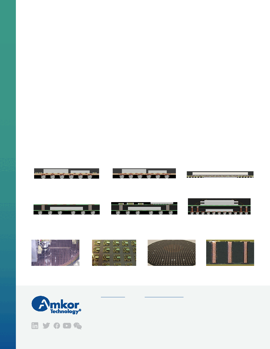 With respect to the information in this document, Amkor makes no guarantee or warranty of its accuracy or that the use of such information will not infringe upon the intellectual rights of third parties. Amkor shall not be responsible for any loss or damage of whatever nature resulting from the use of, or reliance upon it and no patent or other license is implied hereby. This document does not in any way extend or modify Amkor’s warranty on any product beyond that set forth in its standard terms and conditions of sale. Amkor reserves the right to make changes in its product and specifications at any time and without notice. The Amkor name and logo are registered trademarks of Amkor Technology, Inc. All other trademarks mentioned are property of their respective companies. © 2019 Amkor Technology, Incorporated. All Rights Reserved. DS703B-EN Rev Date: 08/19 Visit amkor.com or email sales@amkor.com for more information. Design Features f Package size: 2 x 3 mm2 - 33 x 28 mm2 f Package thickness: 0.275 mm (WLSiP – Multi-chip module) to 1.900 mm (WL3D) f WLSiP with up to 10 active dies and 50 passives qualified f Minimum through package via pitch: 0.350 mm f BGA pitch: down to 0.350 µm f Minimum die-to-die distance: 0.100 mm f Minimum passive-to-die and passive-to-passive distance: 0.150 mm f Minimum die TPV pad pitch: 0.050 mm and opening 0.045 mm f Bottom side Cu-RDL minimum line/space: 0.010 mm/0.010 mm, multi-layer RDL f Top side Cu-RDL minimum line/space: 0.020 mm/0.020 mm, single-layer RDL WLSiP & WL3D Differentiation f High integration density through small die-to-die distance f Multi-layer RDL and double-sided RDL (WLFO bottom and top side) f 3D stacking enabled by TPV concept f Small form factor (optimization based on customer needs in footprint or z-height) f BGA ball attach and flip chip with underfill assembly on same WLFO bottom side f Heterogeneous integration of multiple different active dies (Si, GaAs, SiGe), already packaged dies, passives, optical elements, sensors and MEMS Cross Sections WLFO-Based Embedded Wafer Level System Integration Portfolio WLSiP passives integration WLSiP multi-chip module WL3D face-to-face WL3D RDL on both sides through package vias WLSiP multi-chip module WL3D Package-on-Package, face-to-face, through package vias Dual die package pick & place WLSiP before molding WLSiP after molding Cross section through package vias |
|
|
Link URL |
| Does ALLDATASHEET help your business so far? [ DONATE ] |
About Alldatasheet | Advertisement | Contact us | Privacy Policy | Link to Datasheet | Link Exchange | Manufacturer List All Rights Reserved©Alldatasheet.com |
| Russian : Alldatasheetru.com | Korean : Alldatasheet.co.kr | Spanish : Alldatasheet.es | French : Alldatasheet.fr | Italian : Alldatasheetit.com Portuguese : Alldatasheetpt.com | Polish : Alldatasheet.pl | Vietnamese : Alldatasheet.vn Indian : Alldatasheet.in | Mexican : Alldatasheet.com.mx | British : Alldatasheet.co.uk | New Zealand : Alldatasheet.co.nz |
|
Family Site : ic2ic.com |
icmetro.com |
 British ▼
 English
 Chinese
 German
 Japanese
 Russian
 Korean
 Spanish
 French
 Italian
 Portuguese
 Polish
 Vietnamese
 Indian
 Mexican
 British
 New Zealand


