|
Electronic Components Datasheet Search |
|
|
Electronic Components Datasheet Search |
|
ADPL42002ACPZN-R7 Datasheet(PDF) 7 Page - Analog Devices |
|
|
|||||||||||||||||||||||||||||
ADPL42002ACPZN-R7 Datasheet(HTML) 7 Page - Analog Devices |
|
|
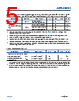
7 / 22 page 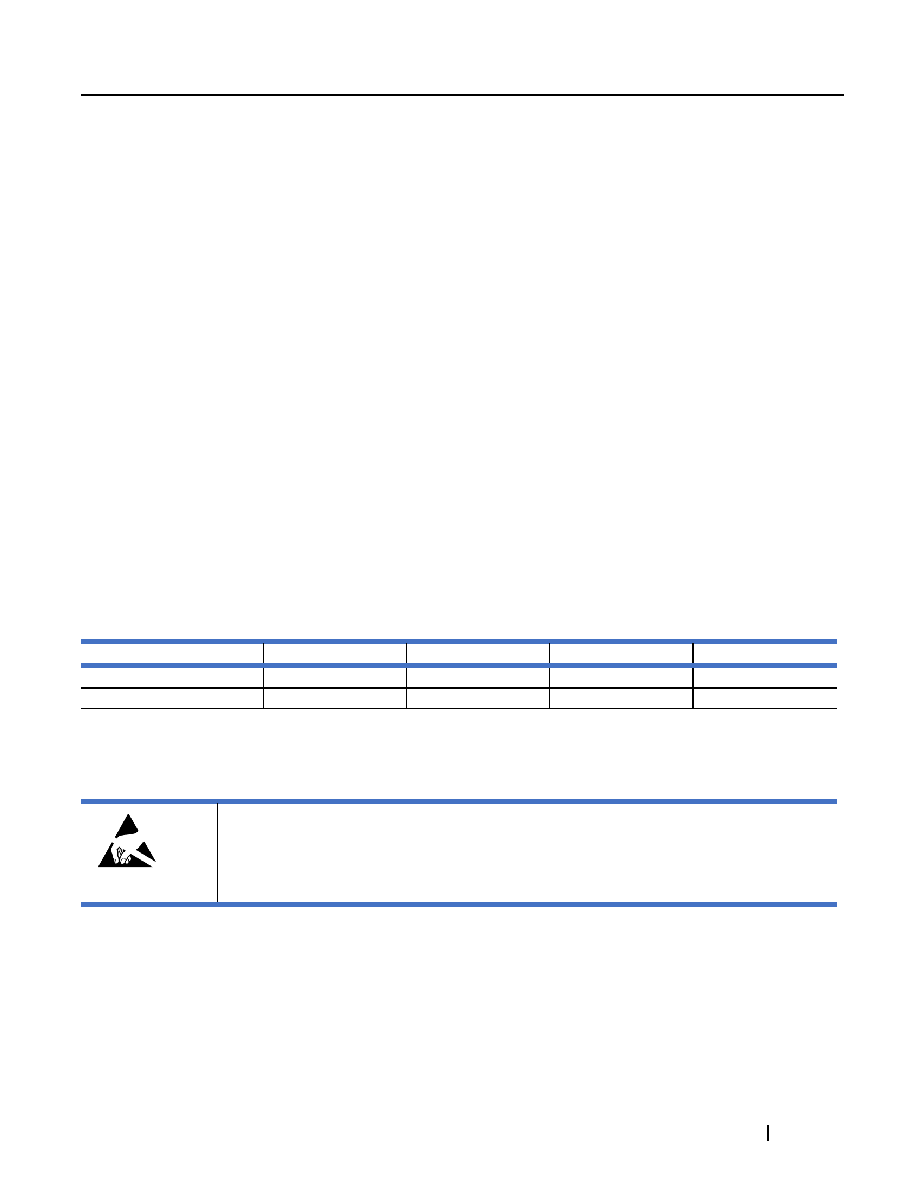 Data Sheet ADPL42002 analog.com Rev. 1 7 of 22 Maximum TJ is calculated from the TA and PD using the formula. TJ = TA + (PD × θJA) (1) θJA of the package is based on modeling and calculation using a 4-layer board. The θJA is highly dependent on the application and board layout. In applications where high maximum power dissipation exists, close attention to thermal board design is required. The value of θJA may vary depending on PCB material, layout, and environmental conditions. The specified values of θJA are based on a 4-layer, 4 inches x 3 inches circuit board. See JESD51-7 and JESD51-9 for detailed information on the board construction. ΨJB is the junction-to-board thermal characterization parameter with units of °C/W. The ΨJB of the package is based on modeling and calculation using a 4-layer board. The JESD51-12, Guidelines for Reporting and Using Electronic Package Thermal Information, states that thermal characterization parameters are not the same as thermal resistances. ΨJB measures the component power flowing through multiple thermal paths rather than a single path, as in thermal resistance (θJB). Therefore, ΨJB thermal paths include convection from the top of the package as well as radiation from the package, factors that make ΨJB more useful in real-world applications. Maximum TJis calculated from the board temperature (TB) and PD using the formula. TJ = TB + (PD × ΨJB) (2) See JESD51-8 and JESD51-12 for more detailed information about ΨJB. Thermal Resistance θJA, θJC, and ΨJB are specified for the worst-case conditions, that is, a device soldered in a circuit board for surface- mount packages. Table 4. Thermal Resistance Package Type θJA θJC ΨJB UNIT 6-Lead LFCSP 72.1 42.3 47.1 °C/W 8-Lead SOIC 52.7 41.5 32.7 °C/W ESD Caution ESD (electrostatic discharge) sensitive device. Charged devices and circuit boards can discharge without detection. Although this product features patented or proprietary protection circuitry, damage may occur on devices subjected to high energy ESD. Therefore, proper ESD precautions should be taken to avoid performance degradation or loss of functionality. |
|
|
Link URL |
| Does ALLDATASHEET help your business so far? [ DONATE ] |
About Alldatasheet | Advertisement | Contact us | Privacy Policy | Link to Datasheet | Link Exchange | Manufacturer List All Rights Reserved©Alldatasheet.com |
| Russian : Alldatasheetru.com | Korean : Alldatasheet.co.kr | Spanish : Alldatasheet.es | French : Alldatasheet.fr | Italian : Alldatasheetit.com Portuguese : Alldatasheetpt.com | Polish : Alldatasheet.pl | Vietnamese : Alldatasheet.vn Indian : Alldatasheet.in | Mexican : Alldatasheet.com.mx | British : Alldatasheet.co.uk | New Zealand : Alldatasheet.co.nz |
|
Family Site : ic2ic.com |
icmetro.com |
 British ▼
 English
 Chinese
 German
 Japanese
 Russian
 Korean
 Spanish
 French
 Italian
 Portuguese
 Polish
 Vietnamese
 Indian
 Mexican
 British
 New Zealand