|
Electronic Components Datasheet Search |
|
|
Electronic Components Datasheet Search |
|
STM32F412RGT3P Datasheet(PDF) 79 Page - STMicroelectronics |
|
|
|||||||||||||||||||||||||||||
STM32F412RGT3P Datasheet(HTML) 79 Page - STMicroelectronics |
|
|
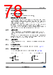
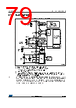
79 / 201 page 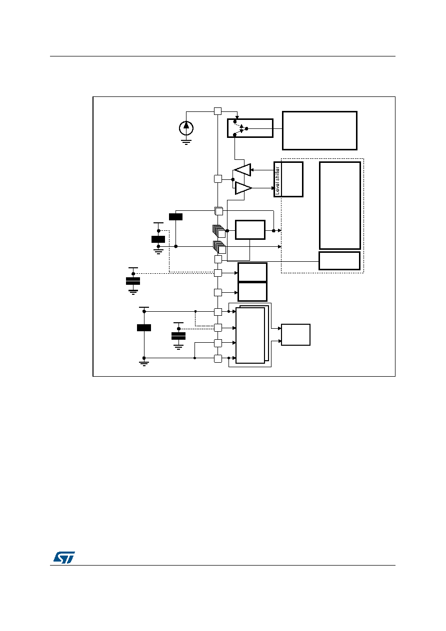 DocID028087 Rev 7 79/201 STM32F412xE/G Electrical characteristics 166 6.1.6 Power supply scheme Figure 21. Power supply scheme 1. To connect PDR_ON pin, refer to Section: Power supply supervisor. 2. The 4.7 µF ceramic capacitor must be connected to one of the VDD pin. 3. VCAP_2 pad is only available on 100-pin and 144-pin packages. 4. VDDA=VDD and VSSA=VSS. 5. VDDUSB is a dedicated independent USB power supply for the on-chip full-speed OTG PHY module and associated DP/DM GPIOs. VDDUSB value does not depend on the VDD and VDDA values, but it must be the last supply to be provided and the first to disappear. Caution: Each power supply pair (for example VDD/VSS, VDDA/VSSA) must be decoupled with filtering ceramic capacitors as shown above. These capacitors must be placed as close as possible to, or below, the appropriate pins on the underside of the PCB to ensure good operation of the device. It is not recommended to remove filtering capacitors to reduce PCB size or cost. This might cause incorrect operation of the device. |
|
Link URL |
| Does ALLDATASHEET help your business so far? [ DONATE ] |
About Alldatasheet | Advertisement | Contact us | Privacy Policy | Link to Datasheet | Link Exchange | Manufacturer List All Rights Reserved©Alldatasheet.com |
| Russian : Alldatasheetru.com | Korean : Alldatasheet.co.kr | Spanish : Alldatasheet.es | French : Alldatasheet.fr | Italian : Alldatasheetit.com Portuguese : Alldatasheetpt.com | Polish : Alldatasheet.pl | Vietnamese : Alldatasheet.vn Indian : Alldatasheet.in | Mexican : Alldatasheet.com.mx | British : Alldatasheet.co.uk | New Zealand : Alldatasheet.co.nz |
|
Family Site : ic2ic.com |
icmetro.com |
 British ▼
 English
 Chinese
 German
 Japanese
 Russian
 Korean
 Spanish
 French
 Italian
 Portuguese
 Polish
 Vietnamese
 Indian
 Mexican
 British
 New Zealand