|
Electronic Components Datasheet Search |
|
|
Electronic Components Datasheet Search |
|
H8SX/1663 Datasheet(PDF) 1021 Page - Renesas Technology Corp |
|
|
|||||||||||||||||||||||||||||
H8SX/1663 Datasheet(HTML) 1021 Page - Renesas Technology Corp |
|
|
1021 / 1158 page 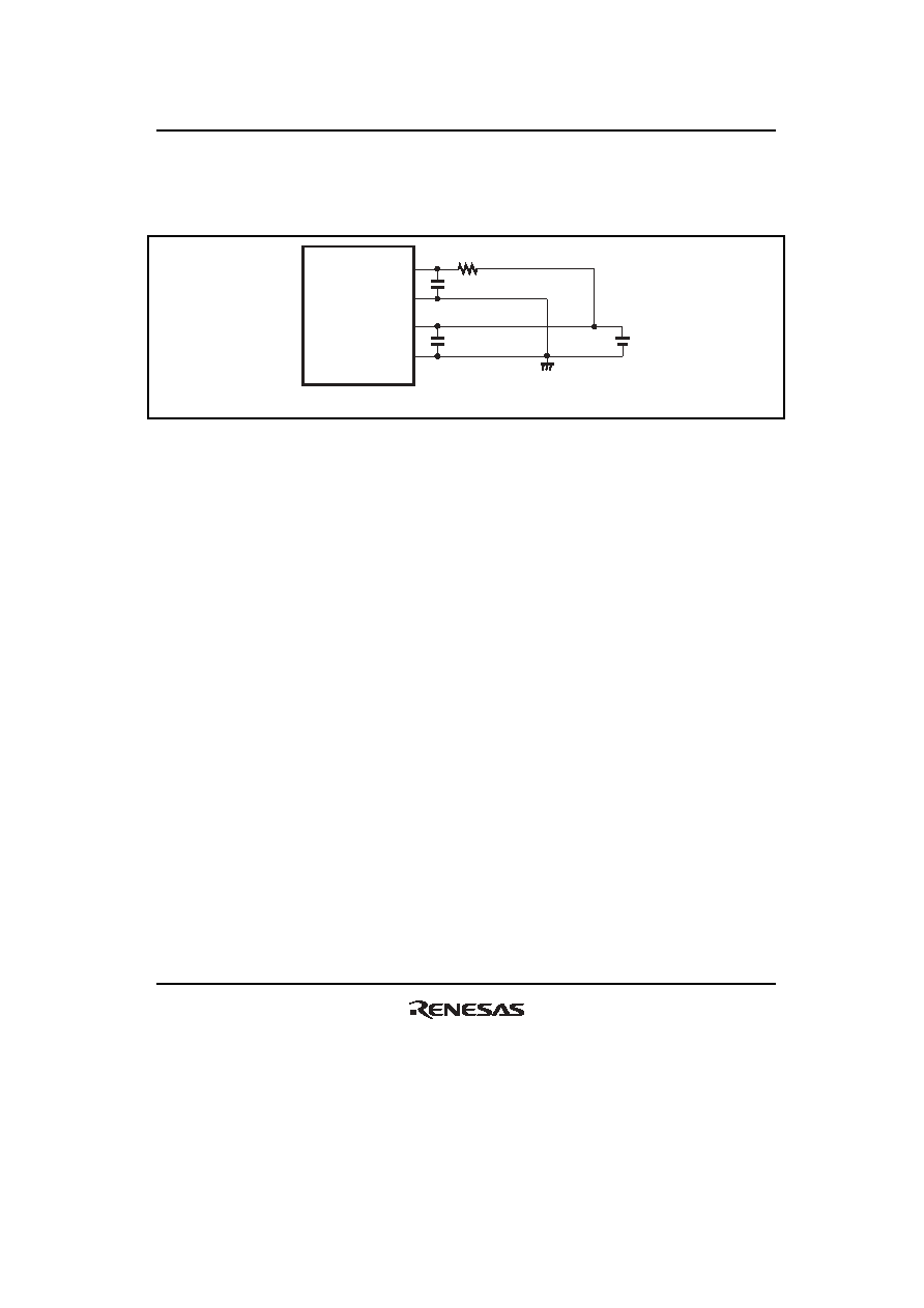 Section 22 Clock Pulse Generator Rev.1.00 Jun. 07, 2006 Page 969 of 1102 REJ09B0294-0100 Figure 22.11 shows the external circuitry recommended for the PLL circuit. Separate PLLVcc and PLLVss from the other Vcc and Vss lines at the board power supply source, and be sure to insert bypass capacitors CPB and CB close to the pins. PLLVCC PLLVSS VCC VSS Rp: 100 Ω CPB: 0.1 µF* CB: 0.1 µF* Note: * CB and CPB are laminated ceramic capacitors. Figure 22.11 Recommended External Circuitry for PLL Circuit |
|
Link URL |
| Does ALLDATASHEET help your business so far? [ DONATE ] |
About Alldatasheet | Advertisement | Contact us | Privacy Policy | Link to Datasheet | Link Exchange | Manufacturer List All Rights Reserved©Alldatasheet.com |
| Russian : Alldatasheetru.com | Korean : Alldatasheet.co.kr | Spanish : Alldatasheet.es | French : Alldatasheet.fr | Italian : Alldatasheetit.com Portuguese : Alldatasheetpt.com | Polish : Alldatasheet.pl | Vietnamese : Alldatasheet.vn Indian : Alldatasheet.in | Mexican : Alldatasheet.com.mx | British : Alldatasheet.co.uk | New Zealand : Alldatasheet.co.nz |
|
Family Site : ic2ic.com |
icmetro.com |
 British ▼
 English
 Chinese
 German
 Japanese
 Russian
 Korean
 Spanish
 French
 Italian
 Portuguese
 Polish
 Vietnamese
 Indian
 Mexican
 British
 New Zealand