|
Electronic Components Datasheet Search |
|
|
Electronic Components Datasheet Search |
|
H8SX/1663M Datasheet(PDF) 978 Page - Renesas Technology Corp |
|
|
|||||||||||||||||||||||||||||
H8SX/1663M Datasheet(HTML) 978 Page - Renesas Technology Corp |
|
|
978 / 1504 page 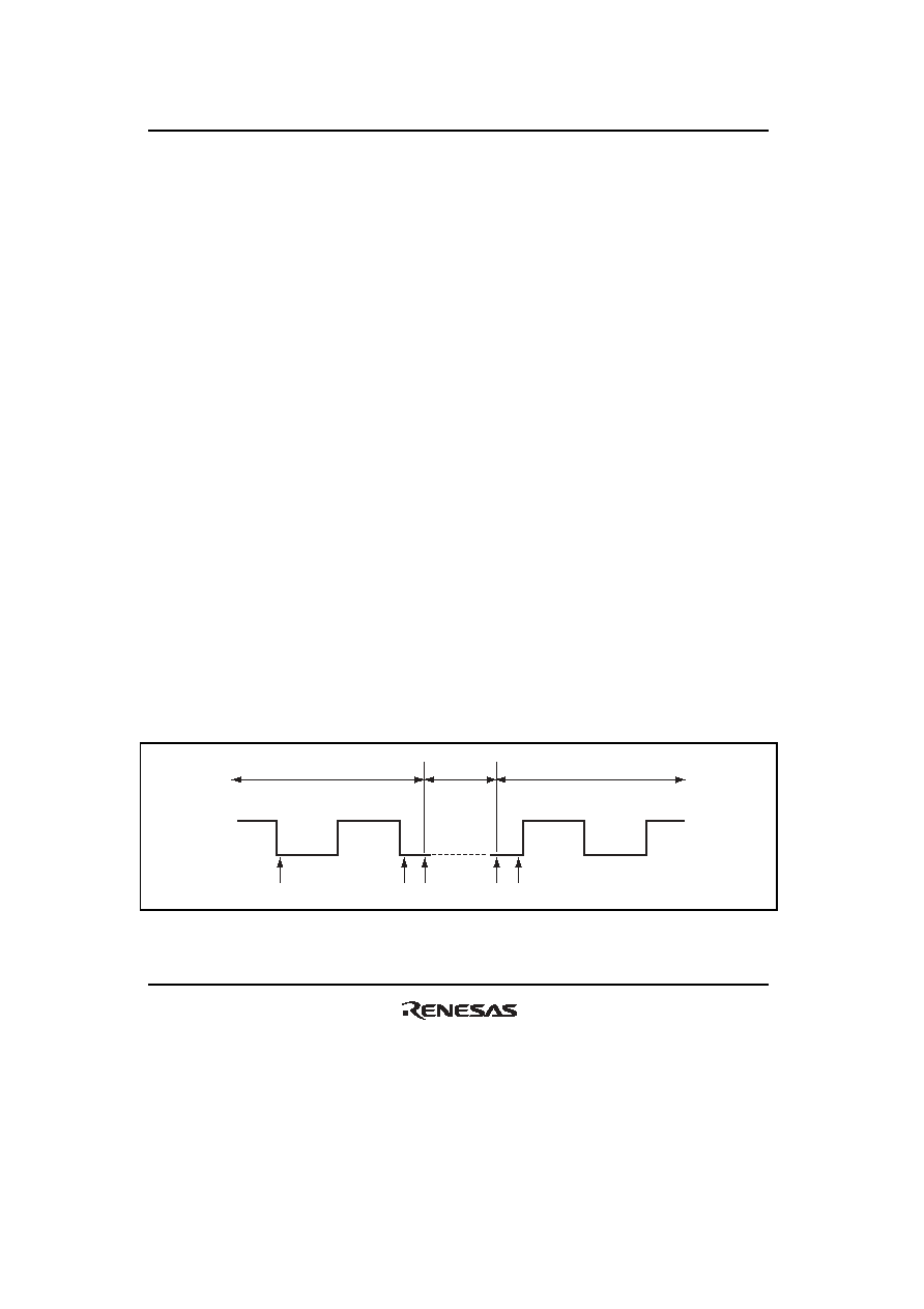 Section 19 Serial Communication Interface (SCI, IrDA, CRC) Rev. 2.00 Sep. 24, 2008 Page 946 of 1468 REJ09B0412-0200 At power-on and transitions to/from software standby mode, use the following procedure to secure the appropriate clock duty cycle. • At power-on To secure the appropriate clock duty cycle simultaneously with power-on, use the following procedure. 1. Initially, port input is enabled in the high-impedance state. To fix the potential level, use a pull-up or pull-down resistor. 2. Fix the SCK pin to the specified output using the CKE1 bit in SCR. 3. Set SMR and SCMR to enable smart card interface mode. Set the CKE0 bit in SCR to 1 to start clock output. • At mode switching At transition from smart card interface mode to software standby mode 1. Set the data register (DR) and data direction register (DDR) corresponding to the SCK pin to the values for the output fixed state in software standby mode. (SCI_0, 1, 2, and 4 only) 2. Write 0 to the TE and RE bits in SCR to stop transmission/reception. Simultaneously, set the CKE1 bit to the value for the output fixed state in software standby mode. 3. Write 0 to the CKE0 bit in SCR to stop the clock. 4. Wait for one cycle of the serial clock. In the mean time, the clock output is fixed to the specified level with the duty cycle retained. 5. Make the transition to software standby mode. At transition from smart card interface mode to software standby mode 1. Clear software standby mode. 2. Write 1 to the CKE0 bit in SCR to start clock output. A clock signal with the appropriate duty cycle is then generated. [1] [2] [3] [4] [5] [7] Software standby Normal operation Normal operation [6] Figure 19.35 Clock Stop and Restart Procedure |
|
Link URL |
| Does ALLDATASHEET help your business so far? [ DONATE ] |
About Alldatasheet | Advertisement | Contact us | Privacy Policy | Link to Datasheet | Link Exchange | Manufacturer List All Rights Reserved©Alldatasheet.com |
| Russian : Alldatasheetru.com | Korean : Alldatasheet.co.kr | Spanish : Alldatasheet.es | French : Alldatasheet.fr | Italian : Alldatasheetit.com Portuguese : Alldatasheetpt.com | Polish : Alldatasheet.pl | Vietnamese : Alldatasheet.vn Indian : Alldatasheet.in | Mexican : Alldatasheet.com.mx | British : Alldatasheet.co.uk | New Zealand : Alldatasheet.co.nz |
|
Family Site : ic2ic.com |
icmetro.com |
 British ▼
 English
 Chinese
 German
 Japanese
 Russian
 Korean
 Spanish
 French
 Italian
 Portuguese
 Polish
 Vietnamese
 Indian
 Mexican
 British
 New Zealand