|
Electronic Components Datasheet Search |
|
|
Electronic Components Datasheet Search |
|
HV441 Datasheet(PDF) 3 Page - Supertex, Inc |
|
|
|||||||||||||||||||||||||||||
HV441 Datasheet(HTML) 3 Page - Supertex, Inc |
|
|
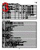
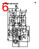
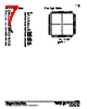
3 / 7 page  3 Pin Description Symbol Parameters Min Typ Max Unit Conditions V PP1 High voltage positive supply 15 110 V T A = -40°C to +85°C V PP2 Positive charge pump output voltage V PP1 – 8 V PP1 – 19 V T A = -40°C to +85°C V NN1 High voltage negative supply V PP – 220 -110 V T A = -40°C to +85°C V NN2 Negative charge pump output voltage V NN1 + 5.2 V NN1 +10.5 V T A = -40°C to +85°C V DD1 Low voltage supply 3.0 5.5 V T A = -40°C to +85°C V DD2 Low voltage supply 10.8 13.5 V T A = -40°C to +85°C I PP1Q V PP1 quiescent current 250 400 µAT A = -40°C to +85°C I NN1Q V NN1 quiescent current 250 500 µAT A = -40°C to +85°C I PP1 V PP1 operating current 0.8 mA HV OUT switching at 100KHz, V PP1 = +60V, VNN1 = -160V, T A = -40°C to +85°C I NN1 V NN1 operating current 1.0 mA I DD1Q V DD1 quiescent current 10 µA I DD2Q V DD2 quiescent current 4.0 mA Electrical Characteristics, cont’d. (Over operating supply voltage unless otherwise specified, TA = 25°C.) V PP1 Positive high voltage supply V PP2 Positive gate voltage supply. Generated by an internal linear regulator. V NN1 Negative high voltage supply V NN2 Negative gate voltage supply. Generated by an internal linear regulator. V DD1 +3.3V to 5.0V supply for input and output logic V DD2 +12V supply for analog/logic circuit GND Low voltage ground P GND High voltage power ground Input1- Inverting input of op-amp 1. Input1+ Noninverting input of op-amp 1. Output1 Output of op-amp 1. Input2- Inverting input of op-amp 2. Input2+ Noninverting input of op-amp 2. Output2 Output of op-amp 2. Input3- Inverting input of op-amp 3. Input3+ Noninverting input of op-amp 3. Output3 Output of op-amp 3. V ref External input reference voltage for zero crossing detection. On/Off Enables/Disables HV OUT. osc1 Input 1 for external resonator. Connect to GND when not in use. osc2 Input 2 for external resonator. Leave floating when not in use. oscin External oscillator input. Zero to V DD1 input signal. Connect to VDD1 when not in use. oscout Oscillator output; 1/4 frequency of external resonator. 50% duty cycle. HV OUT High voltage output. Voltage swings from V PP1 to VNN1. V psen Pulse by pulse over current sensing for internal P-Channel MOSFET. V nsen Pulse by pulse over current sensing for internal N-Channel MOSFET. P gate Gate drive for external P-channel MOSFET. Ngate Gate drive for external N-channel MOSFET. HV441 |
|
|
Link URL |
| Does ALLDATASHEET help your business so far? [ DONATE ] |
About Alldatasheet | Advertisement | Contact us | Privacy Policy | Link to Datasheet | Link Exchange | Manufacturer List All Rights Reserved©Alldatasheet.com |
| Russian : Alldatasheetru.com | Korean : Alldatasheet.co.kr | Spanish : Alldatasheet.es | French : Alldatasheet.fr | Italian : Alldatasheetit.com Portuguese : Alldatasheetpt.com | Polish : Alldatasheet.pl | Vietnamese : Alldatasheet.vn Indian : Alldatasheet.in | Mexican : Alldatasheet.com.mx | British : Alldatasheet.co.uk | New Zealand : Alldatasheet.co.nz |
|
Family Site : ic2ic.com |
icmetro.com |
 British ▼
 English
 Chinese
 German
 Japanese
 Russian
 Korean
 Spanish
 French
 Italian
 Portuguese
 Polish
 Vietnamese
 Indian
 Mexican
 British
 New Zealand