 |
Electronic Components Datasheet Search |
|
|
Electronic Components Datasheet Search |
|
PCF8564A Datasheet(PDF) 33 Page - NXP Semiconductors |
|
|
|||||||||||||||||||||||||||||
PCF8564A Datasheet(HTML) 33 Page - NXP Semiconductors |
|
|
33 / 44 page 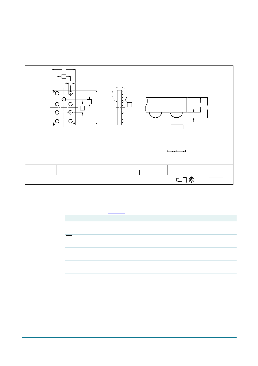 PCF8564A_1 © NXP B.V. 2009. All rights reserved. Product data sheet Rev. 1 — 8 October 2009 33 of 44 NXP Semiconductors PCF8564A Real time clock and calendar Fig 28. Bare die outline of PCF8564ACX9 References Outline version European projection Issue date IEC JEDEC JEITA PCF8564ACX9 pcf8564acx9_po 09-08-25 09-09-09 Unit mm max nom min 0.29 0.09 0.2 1.27 1.9 0.73 0.27 A Dimensions Note 1. Chip dimensions including sawline. 2. Marking code: PC8564A-1 WLCSP9: wafer level chip-size package; 9 bumps; 1.27 x 1.9 x 0.29 mm PCF8564ACX9 A1 A2 0.2 bD(1) E(1) ee1 0.45 e2 0 0.5 1 mm scale X e2 e1 e b D E (2) detail X A1 A2 A y 0,0 x Table 32. Solder bump description for all PCF8564ACX types All x/y coordinates represent the position of the center of each bump with respect to the center (x/y = 0) of the chip; see Figure 28. Symbol Bump X ( µm) Y ( µm) Description OSCI 1 −368 738 oscillator input OSCO 2 −368 188 oscillator output INT 3 −368 −262 open-drain interrupt output (active LOW) VSS 4 −368 −712 ground (substrate) SDA 5 362 −712 serial data I/O SCL 6 362 −262 serial clock input CLKOUT 7 362 188 CMOS push-pull clock output VDD 8 0 456 supply CLKOE 9 362 738 CLKOUT output enable |
|
Link URL |
| Does ALLDATASHEET help your business so far? [ DONATE ] |
About Alldatasheet | Advertisement | Contact us | Privacy Policy | Link to Datasheet | Link Exchange | Manufacturer List All Rights Reserved©Alldatasheet.com |
| Russian : Alldatasheetru.com | Korean : Alldatasheet.co.kr | Spanish : Alldatasheet.es | French : Alldatasheet.fr | Italian : Alldatasheetit.com Portuguese : Alldatasheetpt.com | Polish : Alldatasheet.pl | Vietnamese : Alldatasheet.vn Indian : Alldatasheet.in | Mexican : Alldatasheet.com.mx | British : Alldatasheet.co.uk | New Zealand : Alldatasheet.co.nz |
|
Family Site : ic2ic.com |
icmetro.com |
 British ▼
 English
 Chinese
 German
 Japanese
 Russian
 Korean
 Spanish
 French
 Italian
 Portuguese
 Polish
 Vietnamese
 Indian
 Mexican
 British
 New Zealand


