 |
Electronic Components Datasheet Search |
|
|
Electronic Components Datasheet Search |
|
PCF8564A Datasheet(PDF) 7 Page - NXP Semiconductors |
|
|
|||||||||||||||||||||||||||||
PCF8564A Datasheet(HTML) 7 Page - NXP Semiconductors |
|
|
7 / 45 page 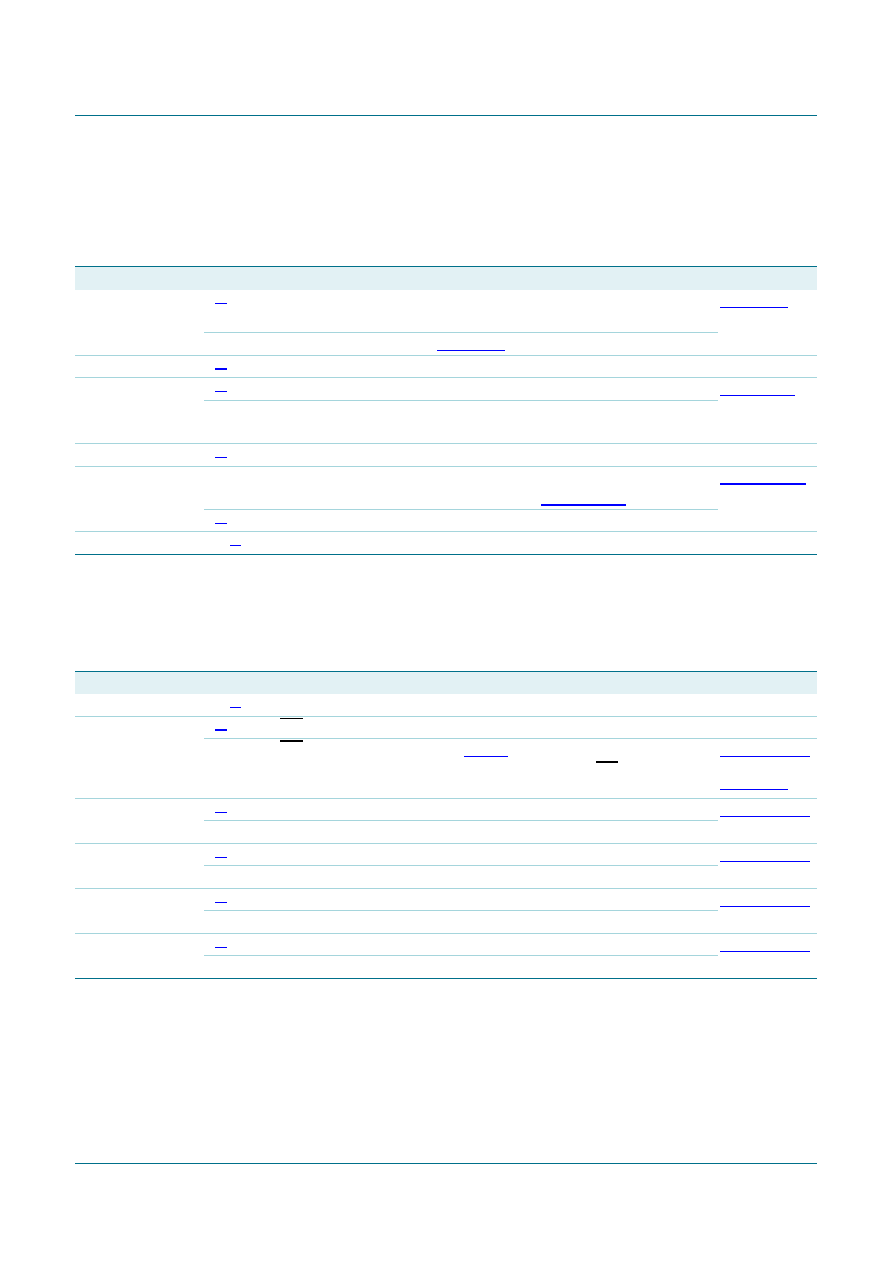 PCF8564A All information provided in this document is subject to legal disclaimers. © NXP B.V. 2010. All rights reserved. Product data sheet Rev. 02 — 30 September 2010 7 of 45 NXP Semiconductors PCF8564A Real time clock and calendar 8.3 Control registers 8.3.1 Register Control_1 [1] Default value. [2] Bits labeled as N should always be written with logic 0. 8.3.2 Register Control_2 [1] Bits labeled as N should always be written with logic 0. [2] Default value. Table 5. Control_1 - control and status register 1 (address 00h) bit description Bit Symbol Value Description Reference 7 TEST1 0[1] normal mode; • must be set to logic 0 during normal operations Section 8.9 1 EXT_CLK test mode (see Section 8.9) 6N 0[2] default value 5STOP 0[1] RTC source clock runs Section 8.10 1 • RTC divider chain flip-flops are asynchronously set to logic 0 • the RTC clock is stopped (CLKOUT at 32.768 kHz is still available) 4N 0[2] default value 3 TESTC 0 Power-On Reset (POR) override facility is disabled; • set to logic 0 for normal operation (see Section 8.11.1) Section 8.11.1 1[1] Power-On Reset (POR) override is enabled 2 to 0 N 000[2] default value Table 6. Control_2 - control and status register 2 (address 01h) bit description Bit Symbol Value Description Reference 7to5 N 000[1] default value 4TI_TP 0[2] INT is active when TF is active (subject to the status of TIE) 1INT pulses active according to Table 7 (subject to the status of TIE); • Remark: note that if AF and AIE are active then INT will be permanently active Section 8.3.2.1 and Section 8.8 3AF 0[2] alarm flag inactive Section 8.3.2.1 1 alarm flag active 2TF 0[2] timer flag inactive Section 8.3.2.1 1 timer flag active 1AIE 0[2] alarm interrupt disabled Section 8.3.2.1 1 alarm interrupt enabled 0TIE 0[2] timer interrupt disabled Section 8.3.2.1 1 timer interrupt enabled |
|
Link URL |
| Does ALLDATASHEET help your business so far? [ DONATE ] |
About Alldatasheet | Advertisement | Contact us | Privacy Policy | Link to Datasheet | Link Exchange | Manufacturer List All Rights Reserved©Alldatasheet.com |
| Russian : Alldatasheetru.com | Korean : Alldatasheet.co.kr | Spanish : Alldatasheet.es | French : Alldatasheet.fr | Italian : Alldatasheetit.com Portuguese : Alldatasheetpt.com | Polish : Alldatasheet.pl | Vietnamese : Alldatasheet.vn Indian : Alldatasheet.in | Mexican : Alldatasheet.com.mx | British : Alldatasheet.co.uk | New Zealand : Alldatasheet.co.nz |
|
Family Site : ic2ic.com |
icmetro.com |
 British ▼
 English
 Chinese
 German
 Japanese
 Russian
 Korean
 Spanish
 French
 Italian
 Portuguese
 Polish
 Vietnamese
 Indian
 Mexican
 British
 New Zealand


