 |
Electronic Components Datasheet Search |
|
|
Electronic Components Datasheet Search |
|
PCF8564AUG Datasheet(PDF) 23 Page - NXP Semiconductors |
|
|
|||||||||||||||||||||||||||||
PCF8564AUG Datasheet(HTML) 23 Page - NXP Semiconductors |
|
|
23 / 48 page 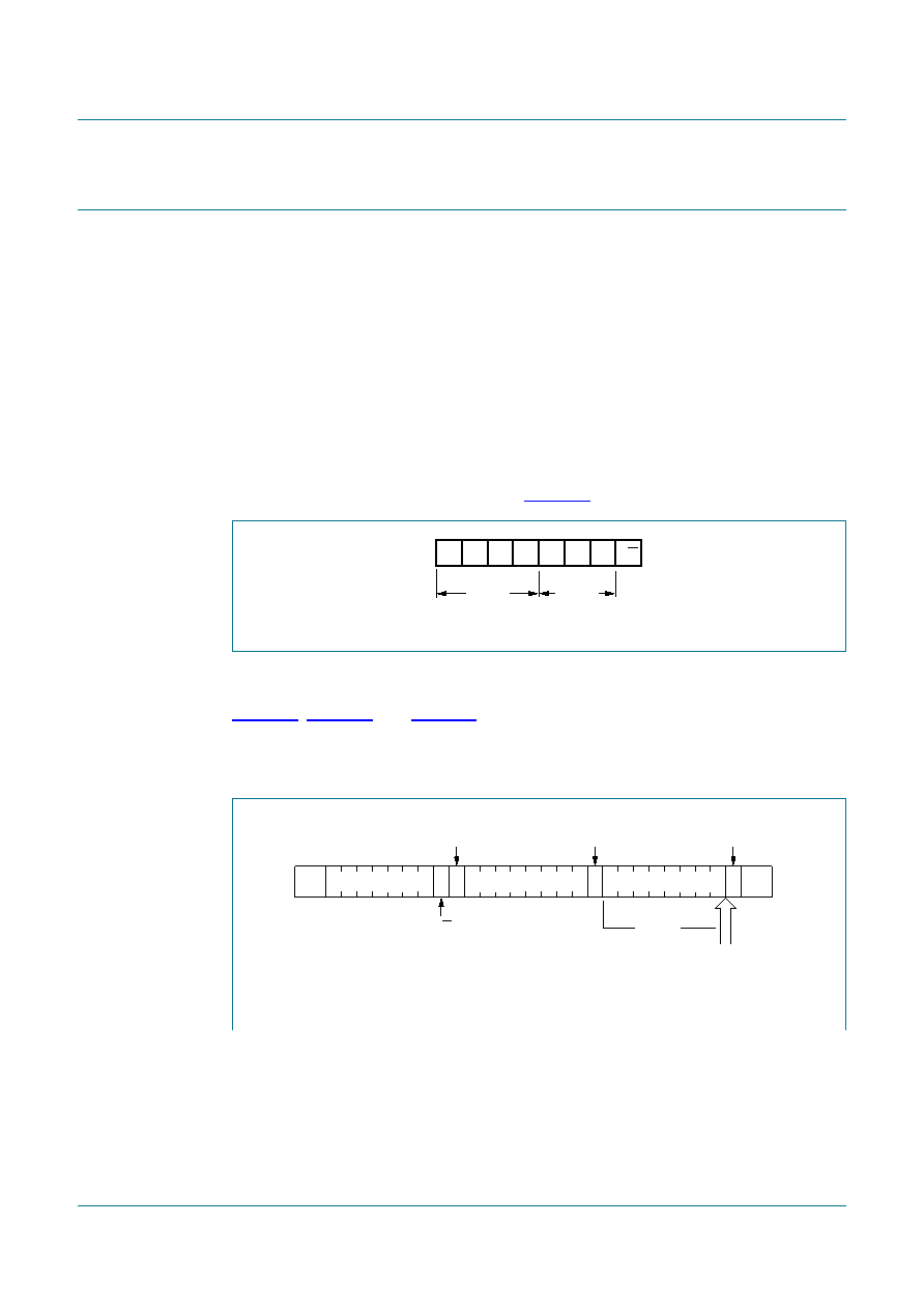 PCF8564A All information provided in this document is subject to legal disclaimers. © NXP B.V. 2013. All rights reserved. Product data sheet Rev. 3 — 26 August 2013 23 of 48 NXP Semiconductors PCF8564A Real time clock and calendar 10. I2C-bus protocol 10.1 Addressing Before any data is transmitted on the I2C-bus, the device which should respond is addressed first. The addressing is always carried out with the first byte transmitted after the start procedure. The PCF8564A acts as a slave receiver or slave transmitter. Therefore, the clock signal SCL is only an input signal, but the data signal SDA is a bidirectional line. Two slave addresses are reserved for the PCF8564A: Read: A3h (1010 0011) Write: A2h (1010 0010) The PCF8564A slave address is shown in Figure 14. 10.2 Clock and calendar READ or WRITE cycles Figure 16, Figure 17, and Figure 18 show the I2C-bus configuration for the different PCF8564A READ and WRITE cycles. The word address is a 4-bit value that defines which register is to be accessed next. The upper four bits of the word address are not used. Fig 15. Slave address Fig 16. Master transmits to slave receiver (WRITE mode) |
|
Link URL |
| Does ALLDATASHEET help your business so far? [ DONATE ] |
About Alldatasheet | Advertisement | Contact us | Privacy Policy | Link to Datasheet | Link Exchange | Manufacturer List All Rights Reserved©Alldatasheet.com |
| Russian : Alldatasheetru.com | Korean : Alldatasheet.co.kr | Spanish : Alldatasheet.es | French : Alldatasheet.fr | Italian : Alldatasheetit.com Portuguese : Alldatasheetpt.com | Polish : Alldatasheet.pl | Vietnamese : Alldatasheet.vn Indian : Alldatasheet.in | Mexican : Alldatasheet.com.mx | British : Alldatasheet.co.uk | New Zealand : Alldatasheet.co.nz |
|
Family Site : ic2ic.com |
icmetro.com |
 British ▼
 English
 Chinese
 German
 Japanese
 Russian
 Korean
 Spanish
 French
 Italian
 Portuguese
 Polish
 Vietnamese
 Indian
 Mexican
 British
 New Zealand


