|
Electronic Components Datasheet Search |
|
|
Electronic Components Datasheet Search |
|
SM8577B Datasheet(PDF) 10 Page - Nippon Precision Circuits Inc |
|
|
|||||||||||||||||||||||||||||
SM8577B Datasheet(HTML) 10 Page - Nippon Precision Circuits Inc |
|
|
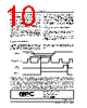
10 / 10 page  SM8577B NIPPON PRECISION CIRCUITS—10 NC9617AE 1997.04 NIPPON PRECISION CIRCUITS INC. NIPPON PRECISION CIRCUITS INC. reserves the right to make changes to the products described in this data sheet in order to improve the design or performance and to supply the best possible products. Nippon Precision Circuits Inc. assumes no responsibility for the use of any circuits shown in this data sheet, conveys no license under any patent or other rights, and makes no claim that the circuits are free from patent infringement. Applications for any devices shown in this data sheet are for illustration only and Nippon Precision Circuits Inc. makes no claim or warranty that such applications will be suitable for the use specified without further testing or modification. The products described in this data sheet are not intended to use for the apparatus which influence human lives due to the failure or malfunction of the products. Customers are requested to comply with applicable laws and regulations in effect now and hereinafter, including compliance with export controls on the distribution or dissemination of the products. Customers shall not export, directly or indirectly, any products without first obtaining required licenses and approvals from appropriate government agencies. NIPPON PRECISION CIRCUITS INC. 4-3, Fukuzumi 2 chome Koto-ku, Tokyo 135-8430, Japan Telephone: 03-3642-6661 Facsimile: 03-3642-6698 When CE is HIGH, data write mode starts from the first rising edge of CLK for which DATA is HIGH. Valid data is then input on DATA from the 9th rising edge of CLK. Time and date data is loaded into the shift register in sync with the rising edge of CLK, starting with the seconds’ digit LSB. Data is loaded and shifted in the sequence second, minute, hour, week, day, and month. After 60 rising edges of CLK, the shift register contents are then transferred to the timer counters. Note that a data write cycle must contain 60 bits of input data. If CE goes LOW before 60 bits are input, the input data is invalid. If the input data exceeds 60 bits, data from the 61st bit is ignored (the first 60 bits remain valid). During a data write cycle, timer counter operation stops on the first falling edge of CLK, and the 1 Hz to 128 Hz frequency divider step counters are reset. The 1 s counter increment signal is stopped and does not restart until CE goes LOW. The divider step counters are reset during the interval between the first falling edge of CLK and the 2nd rising edge of CLK. The data write cycle should be completed within tCE ≤ 0.9 s. If a data read cycle occurs immediately after a data write cycle, a wait time (tRCV) is required after CE goes LOW. Note that activating a read cycle when no valid data is present will cause incorrect operation. All bits must be valid data bits. Supply Voltage Detection The supply voltage detector tests the level of the supply voltage once every 0.5 seconds. If the supply voltage falls below the detector threshold, the FDT bit is set to 1. The FDT bit is reset to 0 after a data read cycle that contains at least 56 data bits. The FDT bit is not reset for data read cycles of 55 bits or less. VDD CE VDET FDT bit (READ MODE) Detected Pulse 0.5 second 0.5 second |
|
|
Link URL |
| Does ALLDATASHEET help your business so far? [ DONATE ] |
About Alldatasheet | Advertisement | Contact us | Privacy Policy | Link to Datasheet | Link Exchange | Manufacturer List All Rights Reserved©Alldatasheet.com |
| Russian : Alldatasheetru.com | Korean : Alldatasheet.co.kr | Spanish : Alldatasheet.es | French : Alldatasheet.fr | Italian : Alldatasheetit.com Portuguese : Alldatasheetpt.com | Polish : Alldatasheet.pl | Vietnamese : Alldatasheet.vn Indian : Alldatasheet.in | Mexican : Alldatasheet.com.mx | British : Alldatasheet.co.uk | New Zealand : Alldatasheet.co.nz |
|
Family Site : ic2ic.com |
icmetro.com |
 British ▼
 English
 Chinese
 German
 Japanese
 Russian
 Korean
 Spanish
 French
 Italian
 Portuguese
 Polish
 Vietnamese
 Indian
 Mexican
 British
 New Zealand