|
Electronic Components Datasheet Search |
|
|
Electronic Components Datasheet Search |
|
NCN5130 Datasheet(PDF) 5 Page - ON Semiconductor |
|
|
|||||||||||||||||||||||||||||
NCN5130 Datasheet(HTML) 5 Page - ON Semiconductor |
|
|
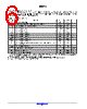
5 / 58 page  NCN5130 www.onsemi.com 5 ELECTRICAL SPECIFICATION Table 2. ABSOLUTE MAXIMUM RATINGS (Notes 1 and 2) Symbol Parameter Min Max Unit VTXO KNX Transmitter Output Voltage −0.3 +45 V ITXO KNX Transmitter Output Current (Note 3) 250 mA VCCP Voltage on CCP−pin −10.5 +14.5 V VCAV Voltage on CAV−pin −0.3 +3.6 V VBUS1 Voltage on VBUS1−pin −0.3 +45 V VANAOUT Voltage on ANAOUT pin −0.3 +3.6 V IBUS1 Current Consumption VBUS1−pin 0 120 mA VCEQ Voltage on pins CEQ1 and CEQ2 −0.3 +45 V VFILT Voltage on VFILT−pin −0.3 +45 V V20V Voltage on V20V−pin −0.3 +25 V VDD2MV Voltage on VDD2MV−pin −0.3 +3.6 V VDD2MC Voltage on VDD2MC−pin −0.3 +45 V VDD2 Voltage on VDD2−pin −0.3 +45 V VSW Voltage on VSW1− and VSW2−pin −0.3 +45 V VIN Voltage on VIN−pin −0.3 +45 V VDD1 Voltage on VDD1−pin −0.3 +3.6 V VDD1M Voltage on VDD1M−pin −0.3 +3.6 V VDIG Voltage on pins MODE1, MODE2, TREQ, CSB/UC1, SDI/TXD, SDO/RXD, SCK/ UC2, XCLK, XSEL, SAVEB, RESETB, XCLKC, TRIG, and FANIN −0.3 +3.6 V VDD Voltage on VDDD− and VDDA−pin −0.3 +3.6 V VXTAL Voltage on XTAL1− and XTAL2−pin −0.3 +3.6 V TST Storage temperature −55 +150 °C TJ Junction Temperature (Note 4) −40 +155 °C VHBM Human Body Model electronic discharge immunity (Note 5) −2 +2 kV Stresses exceeding those listed in the Maximum Ratings table may damage the device. If any of these limits are exceeded, device functionality should not be assumed, damage may occur and reliability may be affected. 1. Convention: currents flowing in the circuit are defined as positive. 2. VBUS2, VSS1, VSS2, VSSA and VSSD form the common ground. They are hard connected to the PCB ground layer. 3. Room temperature, 27 W shunt resistor for transmitter, 250 mA over temperature range. 4. Normal performance within the limitations is guaranteed up to the Thermal Warning level. Between Thermal Warning and Thermal Shutdown temporary loss of function or degradation of performance (which ceases after the disturbance ceases) is possible. 5. According to JEDEC JESD22−A114. |
|
Link URL |
| Does ALLDATASHEET help your business so far? [ DONATE ] |
About Alldatasheet | Advertisement | Contact us | Privacy Policy | Link to Datasheet | Link Exchange | Manufacturer List All Rights Reserved©Alldatasheet.com |
| Russian : Alldatasheetru.com | Korean : Alldatasheet.co.kr | Spanish : Alldatasheet.es | French : Alldatasheet.fr | Italian : Alldatasheetit.com Portuguese : Alldatasheetpt.com | Polish : Alldatasheet.pl | Vietnamese : Alldatasheet.vn Indian : Alldatasheet.in | Mexican : Alldatasheet.com.mx | British : Alldatasheet.co.uk | New Zealand : Alldatasheet.co.nz |
|
Family Site : ic2ic.com |
icmetro.com |
 British ▼
 English
 Chinese
 German
 Japanese
 Russian
 Korean
 Spanish
 French
 Italian
 Portuguese
 Polish
 Vietnamese
 Indian
 Mexican
 British
 New Zealand