|
Electronic Components Datasheet Search |
|
|
Electronic Components Datasheet Search |
|
ADA4937-2YCPZ-R2 Datasheet(PDF) 18 Page - Analog Devices |
|
|
|||||||||||||||||||||||||||||
ADA4937-2YCPZ-R2 Datasheet(HTML) 18 Page - Analog Devices |
|
|
18 / 28 page 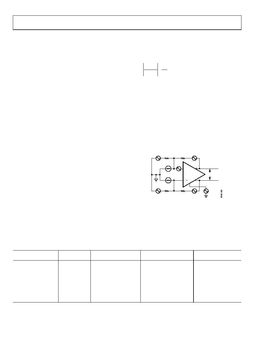 ADA4937-1/ADA4937-2 Data Sheet Rev. F | Page 18 of 28 THEORY OF OPERATION The ADA4937-1/ADA4937-2 differ from conventional operational amplifiers in that they have two outputs whose voltages move in opposite directions. Like an operational amplifier, they rely on open-loop gain and negative feedback to force these outputs to the desired voltages. The ADA4937-1/ADA4937-2 behave much like standard voltage feedback operational amplifiers, which makes it easier to perform single-ended-to-differential conversions, common-mode level shifting, and amplifications of differential signals. Also like an operational amplifier, the ADA4937-1/ADA4937-2 have high input impedance and low output impedance. Two feedback loops control the differential and common-mode output voltages. The differential feedback loop, set with external resistors, controls only the differential output voltage. The common-mode feedback loop controls only the common-mode output voltage. This architecture makes it easy to set the output common-mode level to any arbitrary value. It is forced, by internal common-mode feedback, to be equal to the voltage applied to the VOCM input without affecting the differential output voltage. The ADA4937-1/ADA4937-2 architecture results in outputs that are highly balanced over a wide frequency range without requiring tightly matched external components. The common- mode feedback loop forces the signal component of the output common-mode voltage to zero. This results in nearly perfectly balanced differential outputs that are identical in amplitude and are exactly 180° apart in phase. ANALYZING AN APPLICATION CIRCUIT The ADA4937-1/ADA4937-2 use open-loop gain and negative feedback to force their differential and common-mode output voltages in such a way as to minimize the differential and common-mode error voltages. The differential error voltage is defined as the voltage between the differential inputs labeled +IN and −IN (see Figure 52). For most purposes, this voltage can be assumed to be zero. Similarly, the difference between the actual output common-mode voltage and the voltage applied to VOCM can also be assumed to be zero. Starting from these two assumptions, any application circuit can be analyzed. SETTING THE CLOSED-LOOP GAIN The differential-mode gain of the circuit in Figure 52 can be determined by G F dm IN dm OUT R R V V , , This assumes that the input resistors (RG) and feedback resistors (RF) on each side are equal. ESTIMATING THE OUTPUT NOISE VOLTAGE To estimate the differential output noise of the ADA4937-1/ ADA4937-2 use the noise model in Figure 53. The input-referred noise voltage density, vnIN, is modeled as a differential input, and the noise currents, inIN− and inIN+, appear between each input and ground. The noise currents are assumed to be equal and produce a voltage across the parallel combination of the gain and feedback resistances. vn, cm is the noise voltage density at the VOCM pin. Each of the four resistors contributes (4kTRx)1/2. Table 9 summarizes the input noise sources, the multiplication factors, and the output- referred noise density terms. ADA4937 + RF2 VnOD VnCM VOCM VnIN RF1 RG2 RG1 VnRF1 VnRF2 VnRG1 VnRG2 inIN+ inIN– Figure 53. ADA4937-1/ADA4937-2 Noise Model Table 9. Output Noise Voltage Density Calculations Input Noise Contribution Input Noise Term Input Noise Voltage Density Output Multiplication Factor Output Noise Voltage Density Term Differential Input vnIN vnIN GN vnO1 = GN(vnIN) Inverting Input inIN− inIN− × (RG2||RF2) GN vnO2 = GN[inIN− × (RG2||RF2)] Noninverting Input inIN+ inIN+ × (RG1||RF1) GN vnO3 = GN[inIN+ × (RG1||RF1)] VOCM Input vn, cm vn, cm GN(β1 − β2) vnO4 = GN(β1 − β2)(vn, cm) Gain Resistor RG1 vnRG1 (4kTRG1)1/2 GN(1 − β1) vnO5 = GN(1 − β1)(4kTRG1)1/2 Gain Resistor RG2 vnRG2 (4kTRG2)1/2 GN(1 − β2) vnO6 = GN(1 − β2)(4kTRG2)1/2 Feedback Resistor RF1 vnRF1 (4kTRF1)1/2 1 vnO7 = (4kTRF1)1/2 Feedback Resistor RF2 vnRF2 (4kTRF2)1/2 1 vnO8 = (4kTRF2)1/2 |
|
Link URL |
| Does ALLDATASHEET help your business so far? [ DONATE ] |
About Alldatasheet | Advertisement | Contact us | Privacy Policy | Link to Datasheet | Link Exchange | Manufacturer List All Rights Reserved©Alldatasheet.com |
| Russian : Alldatasheetru.com | Korean : Alldatasheet.co.kr | Spanish : Alldatasheet.es | French : Alldatasheet.fr | Italian : Alldatasheetit.com Portuguese : Alldatasheetpt.com | Polish : Alldatasheet.pl | Vietnamese : Alldatasheet.vn Indian : Alldatasheet.in | Mexican : Alldatasheet.com.mx | British : Alldatasheet.co.uk | New Zealand : Alldatasheet.co.nz |
|
Family Site : ic2ic.com |
icmetro.com |
 British ▼
 English
 Chinese
 German
 Japanese
 Russian
 Korean
 Spanish
 French
 Italian
 Portuguese
 Polish
 Vietnamese
 Indian
 Mexican
 British
 New Zealand