|
Electronic Components Datasheet Search |
|
|
Electronic Components Datasheet Search |
|
M95020-R Datasheet(PDF) 14 Page - STMicroelectronics |
|
|
|||||||||||||||||||||||||||||
M95020-R Datasheet(HTML) 14 Page - STMicroelectronics |
|
|
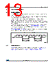
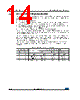
14 / 46 page 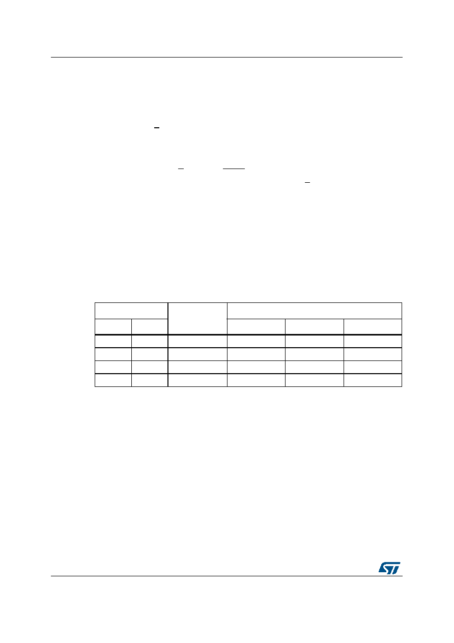 Operating features M950x0-W M950x0-R M950x0-DF 14/46 DocID6512 Rev 13 4.3 Data protection and protocol control To help protect the device from data corruption in noisy or poorly controlled environments, a number of safety features have been built in to the device. The main security measures can be summarized as follows: • WEL bit is reset at power-up. • Chip Select (S) must rise after the eighth clock count (or multiple thereof) in order to start a non-volatile Write cycle (in the memory array or in the Status register). • Accesses to the memory array are ignored during the non-volatile programming cycle, and the programming cycle continues unaffected. • Invalid Chip Select (S) and Hold (HOLD) transitions are ignored. For any instruction to be accepted and executed, Chip Select (S) must be driven high after the rising edge of Serial Clock (C) that latches the last bit of the instruction, and before the next rising edge of Serial Clock (C). For this, “the last bit of the instruction” can be the eighth bit of the instruction code, or the eighth bit of a data byte, depending on the instruction (except in the case of RDSR and READ instructions). Moreover, the “next rising edge of CLOCK” might (or might not) be the next bus transaction for some other device on the bus. When a Write cycle is in progress, the device protects it against external interruption by ignoring any subsequent READ, WRITE or WRSR instruction until the present cycle is complete. Table 3. Write-protected block size Status register bits Protected block Protected array addresses BP1 BP0 M95040 M95020 M95010 0 0 none none none none 0 1 Upper quarter 180h - 1FFh C0h - FFh 60h - 7Fh 1 0 Upper half 100h - 1FFh 80h - FFh 40h - 7Fh 1 1 Whole memory 000h - 1FFh 00h - FFh 00h - 7Fh |
|
Link URL |
| Does ALLDATASHEET help your business so far? [ DONATE ] |
About Alldatasheet | Advertisement | Contact us | Privacy Policy | Link to Datasheet | Link Exchange | Manufacturer List All Rights Reserved©Alldatasheet.com |
| Russian : Alldatasheetru.com | Korean : Alldatasheet.co.kr | Spanish : Alldatasheet.es | French : Alldatasheet.fr | Italian : Alldatasheetit.com Portuguese : Alldatasheetpt.com | Polish : Alldatasheet.pl | Vietnamese : Alldatasheet.vn Indian : Alldatasheet.in | Mexican : Alldatasheet.com.mx | British : Alldatasheet.co.uk | New Zealand : Alldatasheet.co.nz |
|
Family Site : ic2ic.com |
icmetro.com |
 British ▼
 English
 Chinese
 German
 Japanese
 Russian
 Korean
 Spanish
 French
 Italian
 Portuguese
 Polish
 Vietnamese
 Indian
 Mexican
 British
 New Zealand