 |
Electronic Components Datasheet Search |
|
|
Electronic Components Datasheet Search |
|
The question interval is too short.
Please try again in a few seconds.

Hello, Please ask a question about RF5565 Datasheet
# Example questions:
➢ What is the purpose of the lna bypass mode, and what voltage level on the lna_en pin enables it?
➢ Describe the biasing instructions for wifi receive mode. what specific connections must be made, and what should be done with the unused rf ports?
➢ What are the recommended voltage levels for vcc and vreg during wifi transmit mode, and what is the approximate quiescent current expected on vreg?
| Part No. | RF5565 |
| Manufacturer | RFMD |
| Size | 1Mb |
| Pages | 14 pages |
| Description | 2.4GHz TO 2.5GHz, 802.11b/g/n WiFi FRONT END MODULE |






1. Overview
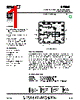
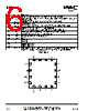
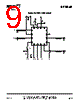
️· Function: The RF5565 is a Front End Module (FEM) designed for 2.4/2.5 GHz WiFi applications. It integrates many components to simplify system design.
️· Applications: Handsets, Personal Media Players, portable battery-powered equipment.
️· Key Features: Integrated matching networks, DC blocking, and a single supply voltage requirement.
2. Core Functionality & Modes of Operation
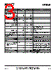
️· WiFi Transmit Mode: Delivers approximately 30dB gain and 20/22dBm output power (depending on modulation). Requires proper biasing (VCC, VREG).
️· WiFi Receive Mode: Provides approximately 14dB gain, 2.2dB Noise Figure (NF), and operates with around 12mA current draw.
️· Bypass Mode (WiFi Receive): Allows direct signal path bypassing the LNA. Useful in certain applications.
️· Bluetooth Mode: Supports Bluetooth operation via an SP3T switch.
3. Key Specifications (Numbers pulled from the text, approximate)
️· Frequency: 2.4 GHz - 2.5 GHz
️· Transmit Gain: ~30 dB
️· Transmit Output Power: 20-22 dBm
️· Receive Gain: ~14 dB
️· Noise Figure (Receive): 2.2 dB
️· Receive Current: ~12 mA
️· Supply Voltage (VCC): 3.3V
️· VREG: (Voltage set to 3.1V, Current ~90mA)
4. Biasing & Control
️· VCC: Main supply voltage.
️· VREG: Controls PA current and bias. Needs careful regulation.
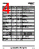
️· C_TX, C_RX, C_BT: Switch control signals to select the desired mode (Transmit, Receive, Bluetooth). These are critical for proper operation.
️· LNA_EN: Enables/Disables the LNA (used for bypass mode).
5. PCB Layout & Application Recommendations
️· 50 Ohm Impedance: All RF traces should be 50 Ohms.
️· Grounding: Adequate grounding is essential for minimizing coupling and heat dissipation.
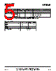
️· Component Values: Critical components (e.g. LNA inductor ~1.2nH) need to be carefully selected.
️· Decoupling Capacitors: Use decoupling capacitors on the supply lines to filter out noise.
️· Thermal Vias: Use thermal vias in the PCB design for proper heat dissipation.
In essence, the RF5565 is a highly integrated solution for WiFi front-end design. Proper PCB layout, careful component selection, and adherence to the biasing recommendations are crucial for achieving optimal performance.
1. Overview
️· Function: The RF5565 is a Front End Module (FEM) designed for 2.4/2.5 GHz WiFi applications. It integrates many components to simplify system design.
️· Applications: Handsets, Personal Media Players, portable battery-powered equipment.
️· Key Features: Integrated matching networks, DC blocking, and a single supply voltage requirement.
2. Core Functionality & Modes of Operation
️· WiFi Transmit Mode: Delivers approximately 30dB gain and 20/22dBm output power (depending on modulation). Requires proper biasing (VCC, VREG).
️· WiFi Receive Mode: Provides approximately 14dB gain, 2.2dB Noise Figure (NF), and operates with around 12mA current draw.
️· Bypass Mode (WiFi Receive): Allows direct signal path bypassing the LNA. Useful in certain applications.
️· Bluetooth Mode: Supports Bluetooth operation via an SP3T switch.
3. Key Specifications (Numbers pulled from the text, approximate)
️· Frequency: 2.4 GHz - 2.5 GHz
️· Transmit Gain: ~30 dB
️· Transmit Output Power: 20-22 dBm
️· Receive Gain: ~14 dB
️· Noise Figure (Receive): 2.2 dB
️· Receive Current: ~12 mA
️· Supply Voltage (VCC): 3.3V
️· VREG: (Voltage set to 3.1V, Current ~90mA)
4. Biasing & Control
️· VCC: Main supply voltage.
️· VREG: Controls PA current and bias. Needs careful regulation.
️· C_TX, C_RX, C_BT: Switch control signals to select the desired mode (Transmit, Receive, Bluetooth). These are critical for proper operation.
️· LNA_EN: Enables/Disables the LNA (used for bypass mode).
5. PCB Layout & Application Recommendations
️· 50 Ohm Impedance: All RF traces should be 50 Ohms.
️· Grounding: Adequate grounding is essential for minimizing coupling and heat dissipation.
️· Component Values: Critical components (e.g. LNA inductor ~1.2nH) need to be carefully selected.
️· Decoupling Capacitors: Use decoupling capacitors on the supply lines to filter out noise.
️· Thermal Vias: Use thermal vias in the PCB design for proper heat dissipation.
In essence, the RF5565 is a highly integrated solution for WiFi front-end design. Proper PCB layout, careful component selection, and adherence to the biasing recommendations are crucial for achieving optimal performance.
| Part No. | RF5565 |
| Manufacturer | RFMD |
| Size | 1Mb |
| Pages | 14 pages |
| Description | 2.4GHz TO 2.5GHz, 802.11b/g/n WiFi FRONT END MODULE |
| Does ALLDATASHEET help your business so far? [ DONATE ] |
About Alldatasheet | Advertisement | Contact us | Privacy Policy | Link to Datasheet | Link Exchange | Manufacturer List All Rights Reserved©Alldatasheet.com |
| Russian : Alldatasheetru.com | Korean : Alldatasheet.co.kr | Spanish : Alldatasheet.es | French : Alldatasheet.fr | Italian : Alldatasheetit.com Portuguese : Alldatasheetpt.com | Polish : Alldatasheet.pl | Vietnamese : Alldatasheet.vn Indian : Alldatasheet.in | Mexican : Alldatasheet.com.mx | British : Alldatasheet.co.uk | New Zealand : Alldatasheet.co.nz |
|
Family Site : ic2ic.com |
icmetro.com |
 British ▼
  English
 Chinese
 German
 Japanese
 Russian
 Korean
 Spanish
 French
 Italian
 Portuguese
 Polish
 Vietnamese
 Indian
 Mexican
 New Zealand