|
Electronic Components Datasheet Search |
|
|
Electronic Components Datasheet Search |
|
SIT1602B Datasheet(PDF) 2 Page - SiTime Corp. |
|
|
|||||||||||||||||||||||||||||
SIT1602B Datasheet(HTML) 2 Page - SiTime Corp. |
|
|
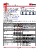
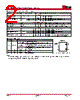
2 / 17 page  SiT1602B Low Power, Standard Frequency Oscillator Rev 1.04 Page 2 of 17 www.sitime.com Table 1. Electrical Characteristics (continued) Parameters Symbol Min. Typ. Max. Unit Condition Input Characteristics Input High Voltage VIH 70% – – Vdd Pin 1, OE or ST ̅ ̅ ̅ Input Low Voltage VIL – – 30% Vdd Pin 1, OE or ST ̅ ̅ ̅ Input Pull-up Impedance Z_in 50 87 150 k Pin 1, OE logic high or logic low, or ST ̅ ̅ ̅ logic high 2 – – M Pin 1, ST ̅ ̅ ̅ logic low Startup and Resume Timing Startup Time T_start – – 5 ms Measured from the time Vdd reaches its rated minimum value Enable/Disable Time T_oe – – 138 ns f = 77.76 MHz. For other frequencies, T_oe = 100 ns + 3 * cycles Resume Time T_resume – – 5 ms Measured from the time ST ̅ ̅ ̅ pin crosses 50% threshold Jitter RMS Period Jitter T_jitt – 1.8 3 ps f = 75 MHz, Vdd = 2.5V, 2.8V, 3.0V or 3.3V – 1.8 3 ps f = 75 MHz, Vdd = 1.8V Peak-to-peak Period Jitter T_pk – 12 25 ps f = 75 MHz, Vdd = 2.5V, 2.8V, 3.0V or 3.3V – 14 30 ps f = 75 MHz, Vdd = 1.8V RMS Phase Jitter (random) T_phj – 0.5 0.9 ps f = 75 MHz, Integration bandwidth = 900 kHz to 7.5 MHz – 1.3 2 ps f = 75 MHz, Integration bandwidth = 12 kHz to 20 MHz Table 2. Pin Description Pin Symbol Functionality 1 OE/ ST ̅ ̅ ̅ /NC Output Enable H [1] : specified frequency output L: output is high impedance. Only output driver is disabled. Standby H [1] : specified frequency output L: output is low (weak pull down). Device goes to sleep mode. Supply current reduces to I_std. No Connect Any voltage between 0 and Vdd or Open [1] : Specified frequency output. Pin 1 has no function. 2 GND Power Electrical ground 3 OUT Output Oscillator output 4 VDD Power Power supply voltage [2] Top View Figure 1. Pin Assignments Notes: 1. In OE or ST ̅ ̅ ̅ mode, a pull-up resistor of 10 kΩ or less is recommended if pin 1 is not externally driven. If pin 1 needs to be left floating, use the NC option. 2. A capacitor of value 0.1 µF or higher between Vdd and GND is required. OE/ST/NC GND OUT VDD |
|
|
Link URL |
| Does ALLDATASHEET help your business so far? [ DONATE ] |
About Alldatasheet | Advertisement | Contact us | Privacy Policy | Link to Datasheet | Link Exchange | Manufacturer List All Rights Reserved©Alldatasheet.com |
| Russian : Alldatasheetru.com | Korean : Alldatasheet.co.kr | Spanish : Alldatasheet.es | French : Alldatasheet.fr | Italian : Alldatasheetit.com Portuguese : Alldatasheetpt.com | Polish : Alldatasheet.pl | Vietnamese : Alldatasheet.vn Indian : Alldatasheet.in | Mexican : Alldatasheet.com.mx | British : Alldatasheet.co.uk | New Zealand : Alldatasheet.co.nz |
|
Family Site : ic2ic.com |
icmetro.com |
 British ▼
 English
 Chinese
 German
 Japanese
 Russian
 Korean
 Spanish
 French
 Italian
 Portuguese
 Polish
 Vietnamese
 Indian
 Mexican
 British
 New Zealand