|
Electronic Components Datasheet Search |
|
|
Electronic Components Datasheet Search |
|
AD9739-R2-EBZ Datasheet(PDF) 34 Page - Analog Devices |
|
|
|||||||||||||||||||||||||||||
AD9739-R2-EBZ Datasheet(HTML) 34 Page - Analog Devices |
|
|
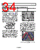
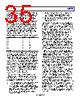
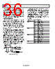
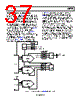
34 / 50 page 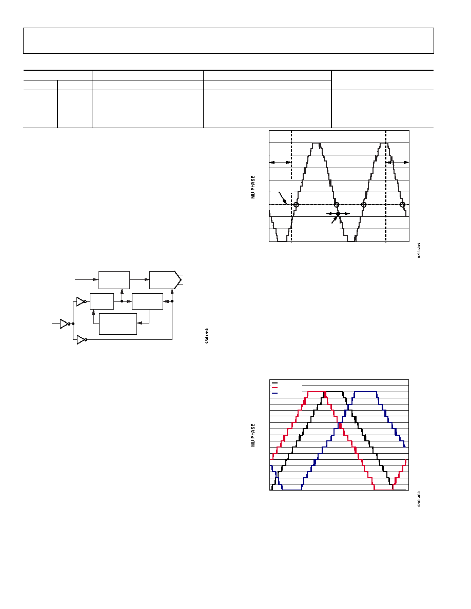 AD9739 Data Sheet Rev. E | Page 34 of 50 Table 27. Example of LVDS Input Levels Applied Voltages Resulting Differential Voltage Resulting Common-Model Voltage VP (V) VN (V) VP, N VCOM Logic Bit Binary Equivalent 1.4 1.0 +0.4 V 1.2 V 1 1.0 1.4 −0.4 V 1.2 V 0 1.0 0.8 +200 mV 900 mV 1 0.8 1.0 −200 mV 900 mV 0 MU CONTROLLER A delay lock loop (DLL) is used to optimize the timing between the internal digital and analog domains of the AD9739 such that data is successfully transferred into the TxDAC core at rates of up to 2.5 GSPS. As shown in Figure 48, the DAC clock is split into an analog and a digital path with the critical analog path leading to the DAC core (for minimum jitter degradation) and the digital path leading to a programmable delay line. Note that the output of this delay line serves as the master internal digital clock from which all other internal and external digital clocks are derived. The amount of delay added to this path is under the control of the mu controller, which optimizes the timing between these two clock domains and continuously tracks any variation (once in track mode) to ensure proper data hand-off. 14-BIT DATA 14-BIT DATA IOUTP IOUTN DIGITAL CIRCUITRY ANALOG CIRCUITRY MU DELAY DAC CLOCK PHASE DETECTOR MU DELAY CONTROLLER Figure 48. Mu Delay Controller Block Diagram The mu controller adjusts the timing relationship between the digital and analog domains via a tapped digital delay line having a nominal total delay of 864 ps. The delay value is programmable to a 9-bit resolution (that is, 0 to 432 decimal) via the MUDEL register, resulting in a nominal resolution of 2 ps/LSB. Because a time delay maps to a phase offset for a fixed clock frequency, the control loop essentially compares the phase relationship between the two clock domains and adjusts the phase (that is, via a tapped delay line) of the digital clock such that it is at the desired fixed phase offset (SET_PHS) from the critical analog clock. 0 2 4 6 8 10 12 14 16 18 0 40 80 120 160 200 240 280 320 360 400 440 SEARCH STARTING LOCATION GUARD BAND GUARD BAND MU DELAY DESIRED PHASE Figure 49. Typical Mu Phase Characteristic Plot at 2.4 GSPS Figure 49 maps the typical mu phase characteristic at 2.4 GSPS vs. the 9-bit digital delay setting (MUDEL). The mu phase scaling is such that a value of 16 corresponds to 180 degrees. The critical keep-out window between the digital and analog domains occurs at a value of 0 (but can extend out to 2 depending on the clock rate). The target mu phase (and slope) is selected to provide optimum ac performance while ensuring that the mu controller for any device can establish and maintain lock. For example, while a slope and phase setting of −6 is considered optimum for operation between 1.6 GSPS and 2.5 GSPS, other values are required below 1.6 GSPS. 0 2 4 6 8 10 12 14 16 18 0 40 80 120 160 200 240 280 320 360 400 440 DELAY LINE TAP NOM_P1 SLOW_P1 FAST_P1 Figure 50. Mu Phase Characteristics of Three Devices from Different Process Lots at 1.2 GSPS |
|
Link URL |
| Does ALLDATASHEET help your business so far? [ DONATE ] |
About Alldatasheet | Advertisement | Contact us | Privacy Policy | Link to Datasheet | Link Exchange | Manufacturer List All Rights Reserved©Alldatasheet.com |
| Russian : Alldatasheetru.com | Korean : Alldatasheet.co.kr | Spanish : Alldatasheet.es | French : Alldatasheet.fr | Italian : Alldatasheetit.com Portuguese : Alldatasheetpt.com | Polish : Alldatasheet.pl | Vietnamese : Alldatasheet.vn Indian : Alldatasheet.in | Mexican : Alldatasheet.com.mx | British : Alldatasheet.co.uk | New Zealand : Alldatasheet.co.nz |
|
Family Site : ic2ic.com |
icmetro.com |
 British ▼
 English
 Chinese
 German
 Japanese
 Russian
 Korean
 Spanish
 French
 Italian
 Portuguese
 Polish
 Vietnamese
 Indian
 Mexican
 British
 New Zealand