|
Electronic Components Datasheet Search |
|
|
Electronic Components Datasheet Search |
|
X9400 Datasheet(PDF) 11 Page - Intersil Corporation |
|
|
|||||||||||||||||||||||||||||
X9400 Datasheet(HTML) 11 Page - Intersil Corporation |
|
|
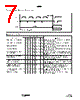
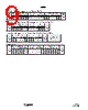
11 / 21 page  11 FN8189.1 March 31, 2005 D.C. OPERATING CHARACTERISTICS (Over the recommended operating conditions unless otherwise specified.) ENDURANCE AND DATA RETENTION CAPACITANCE POWER-UP TIMING POWER-UP REQUIREMENTS (Power-up sequencing can affect correct recall of the wiper registers) The preferred power-on sequence is as follows: First VCC, then the potentiometer pins, RH, RL, and RW. Voltage should not be applied to the potentiometer pins before V+ or V- is applied. The VCC ramp rate specifi-cation should be met, and any glitches or slope changes in the VCC line should be held to <100mV if possible. If VCC powers down, it should be held below 0.1V for more than 1 second before powering up again in order for proper wiper register recall. Also, VCC should not reverse polarity by more than 0.5V. Recall of wiper position will not be complete until VCC, V+ and V-reach their final value. EQUIVALENT A.C. LOAD CIRCUIT Symbol Parameter Limits Test Conditions Min. Typ. Max. Units ICC1 VCC supply current (Active) 400 µA fSCK = 2MHz, SO = Open, Other Inputs = VSS ICC2 VCC supply current (Nonvolatile Write) 1mA fSCK = 2MHz, SO = Open, Other Inputs = VSS ISB VCC current (standby) 1 µA SCK = SI = VSS, Addr. = VSS ILI Input leakage current 10 µA VIN = VSS to VCC ILO Output leakage current 10 µA VOUT = VSS to VCC VIH Input HIGH voltage VCC x 0.7 VCC + 0.5 V VIL Input LOW voltage -0.5 VCC x 0.1 V VOL Output LOW voltage 0.4 V IOL = 3mA Parameter Min. Unit Minimum endurance 100,000 Data changes per bit per register Data retention 100 years Symbol Test Max. Unit Test Conditions COUT (4) Output capacitance (SO) 8 pF VOUT = 0V CIN (4) Input capacitance (A0, A1, SI, and SCK) 6 pF VIN = 0V Symbol Parameter Min. Max. Unit tPUR (5) Power-up to initiation of read operation 1 ms tPUW (5) Power-up to initiation of write operation 5 ms tR VCC (4) VCC Power-up ramp 0.2 50 V/msec 5V 1533 Ω 100pF SDA Output X9400 |
|
|
Link URL |
| Does ALLDATASHEET help your business so far? [ DONATE ] |
About Alldatasheet | Advertisement | Contact us | Privacy Policy | Link to Datasheet | Link Exchange | Manufacturer List All Rights Reserved©Alldatasheet.com |
| Russian : Alldatasheetru.com | Korean : Alldatasheet.co.kr | Spanish : Alldatasheet.es | French : Alldatasheet.fr | Italian : Alldatasheetit.com Portuguese : Alldatasheetpt.com | Polish : Alldatasheet.pl | Vietnamese : Alldatasheet.vn Indian : Alldatasheet.in | Mexican : Alldatasheet.com.mx | British : Alldatasheet.co.uk | New Zealand : Alldatasheet.co.nz |
|
Family Site : ic2ic.com |
icmetro.com |
 British ▼
 English
 Chinese
 German
 Japanese
 Russian
 Korean
 Spanish
 French
 Italian
 Portuguese
 Polish
 Vietnamese
 Indian
 Mexican
 British
 New Zealand