|
Electronic Components Datasheet Search |
|
|
Electronic Components Datasheet Search |
|
TJA1124 Datasheet(PDF) 8 Page - NXP Semiconductors |
|
|
|||||||||||||||||||||||||||||
TJA1124 Datasheet(HTML) 8 Page - NXP Semiconductors |
|
|
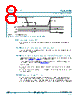
8 / 23 page  NXP Semiconductors TJA1124 Quad LIN master transceiver TJA1124 All information provided in this document is subject to legal disclaimers. © NXP B.V. 2018. All rights reserved. Product data sheet Rev. 1 — 8 May 2018 8 / 23 aaa-029902 twake(dom)LIN VLINx Standby Standby LIN dominant VBUSdom VBUSrec LIN recessive ground HIGH(1) LOW RXDx mode (1) RXDx HIGH level depends on VIO. Figure 5. Principle of remote wake-up via LIN bus in Standby mode 6.3.2 Local wake-up via pin SLP A LOW level on pin SLP lasting at least twake(low)SLP is interpreted as a local wake-up request. 6.4 Operation during automotive cranking pulses The TJA1124 remains fully operational during automotive cranking pulses because it is specified down to VBAT = 5 V. 6.5 Operation when supply voltage is outside specified operating range If VBAT > 28 V or VBAT < 5 V, the TJA1124 may remain operational, but parameter values (as specified in Table 5 and Table 6) cannot be guaranteed. If the voltage on pin BAT drops below the power-off detection threshold, Vth(det)poff, the TJA1124 switches to Off mode (see Section 6.2.1). In Normal mode: • If the input level on pin LINx is recessive, the respective receiver output on pin RXDx will be HIGH. • If the input level on pin TXDx is HIGH, the respective LIN transmitter ouput on pin LINx will be recessive. 6.6 TXD dominant time-out function Once a transmitter has been enabled, its TXD dominant timeout timer is started every time the associated TXD pin goes LOW. If the LOW state on TXDx persists for longer than the TXD dominant timeout time (tto(dom)TXD), the transmitter is disabled, releasing the bus line to recessive state. The TXD dominant timeout timer is reset when pin TXDx goes HIGH. |
|
|
Link URL |
| Does ALLDATASHEET help your business so far? [ DONATE ] |
About Alldatasheet | Advertisement | Contact us | Privacy Policy | Link to Datasheet | Link Exchange | Manufacturer List All Rights Reserved©Alldatasheet.com |
| Russian : Alldatasheetru.com | Korean : Alldatasheet.co.kr | Spanish : Alldatasheet.es | French : Alldatasheet.fr | Italian : Alldatasheetit.com Portuguese : Alldatasheetpt.com | Polish : Alldatasheet.pl | Vietnamese : Alldatasheet.vn Indian : Alldatasheet.in | Mexican : Alldatasheet.com.mx | British : Alldatasheet.co.uk | New Zealand : Alldatasheet.co.nz |
|
Family Site : ic2ic.com |
icmetro.com |
 British ▼
 English
 Chinese
 German
 Japanese
 Russian
 Korean
 Spanish
 French
 Italian
 Portuguese
 Polish
 Vietnamese
 Indian
 Mexican
 British
 New Zealand