|
Electronic Components Datasheet Search |
|
|
Electronic Components Datasheet Search |
|
WM8816 Datasheet(PDF) 11 Page - Wolfson Microelectronics plc |
|
|
|||||||||||||||||||||||||||||
WM8816 Datasheet(HTML) 11 Page - Wolfson Microelectronics plc |
|
|
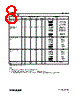
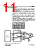
11 / 13 page  Product Preview WM8816 w PP Rev 1.5 October 2004 11 APPLICATION RECOMMENDATIONS 1. For best audio performance, all digital activities should be minimised during analogue signal processing. Special attention should be paid to power and ground decoupling. Decoupling capacitors should be located as close to the WM8816 as possible. A clean analogue power supply should always be used. 2. Damage can be caused to the internal delay generators if AVDD and DVDD supply voltages differ to any degree. The AVDD and DVDD pins must therefore be tied together in all designs. 3. During operation of the hardware MUTEB function between setting mute and then un-mute, the device may either not un-mute or the gain setting after un-mute will be incorrect. It is advised to re-write the gain settings immediately following hardware un-mute to guarantee faultless operation. 4. Voltage greater than 500mV on the digital pins while the device is powered down may prevent successful POR of the device when power is re-applied. It is preferable that all digital pins are pulled low during power up or alternatively ensure that there are no residual voltages held on the digital pins during power down. 5. The WM8816 output offset voltage can vary dependent upon the op-amp used usually with the largest level of offset voltage occurring at +15.5dB gain. Output offset voltage has linear relationship on input bias current and offset voltage amplitudes. Using differing op-amp types causes a large variation in offset voltage. Below is a list of recommended op-amps which are found to give the least offset issues when used with the WM8816. Channel matching is also important factor and not necessarily only the absolute offset value. DEVICE MANUFACTURER OFFSET IN MV OP275 Analog Devices 8.55 MC33078/9 On-Semi/ST 28.4 AD8610 Analog Devices 1.49 LT1793 Linear 18.5 OP1177 Analog Devices 0.505 OP277 BurrBrown 0.228 Table 3 Recommended Op-amps RIN RMO WM8816 DAC Balanced Output + - RFO RGND 15 14 13 12 LIN LMO + - LFO LGND 2 3 4 5 +18V +18V -18V -18V + - +18V -18V 2K 2K 2K 2K Figure 6 Configuration for Double Balanced Output (One Channel) |
|
|
Link URL |
| Does ALLDATASHEET help your business so far? [ DONATE ] |
About Alldatasheet | Advertisement | Contact us | Privacy Policy | Link to Datasheet | Link Exchange | Manufacturer List All Rights Reserved©Alldatasheet.com |
| Russian : Alldatasheetru.com | Korean : Alldatasheet.co.kr | Spanish : Alldatasheet.es | French : Alldatasheet.fr | Italian : Alldatasheetit.com Portuguese : Alldatasheetpt.com | Polish : Alldatasheet.pl | Vietnamese : Alldatasheet.vn Indian : Alldatasheet.in | Mexican : Alldatasheet.com.mx | British : Alldatasheet.co.uk | New Zealand : Alldatasheet.co.nz |
|
Family Site : ic2ic.com |
icmetro.com |
 British ▼
 English
 Chinese
 German
 Japanese
 Russian
 Korean
 Spanish
 French
 Italian
 Portuguese
 Polish
 Vietnamese
 Indian
 Mexican
 British
 New Zealand