|
Electronic Components Datasheet Search |
|
|
Electronic Components Datasheet Search |
|
SC2453 Datasheet(PDF) 11 Page - Semtech Corporation |
|
|
|||||||||||||||||||||||||||||
SC2453 Datasheet(HTML) 11 Page - Semtech Corporation |
|
|
11 / 22 page 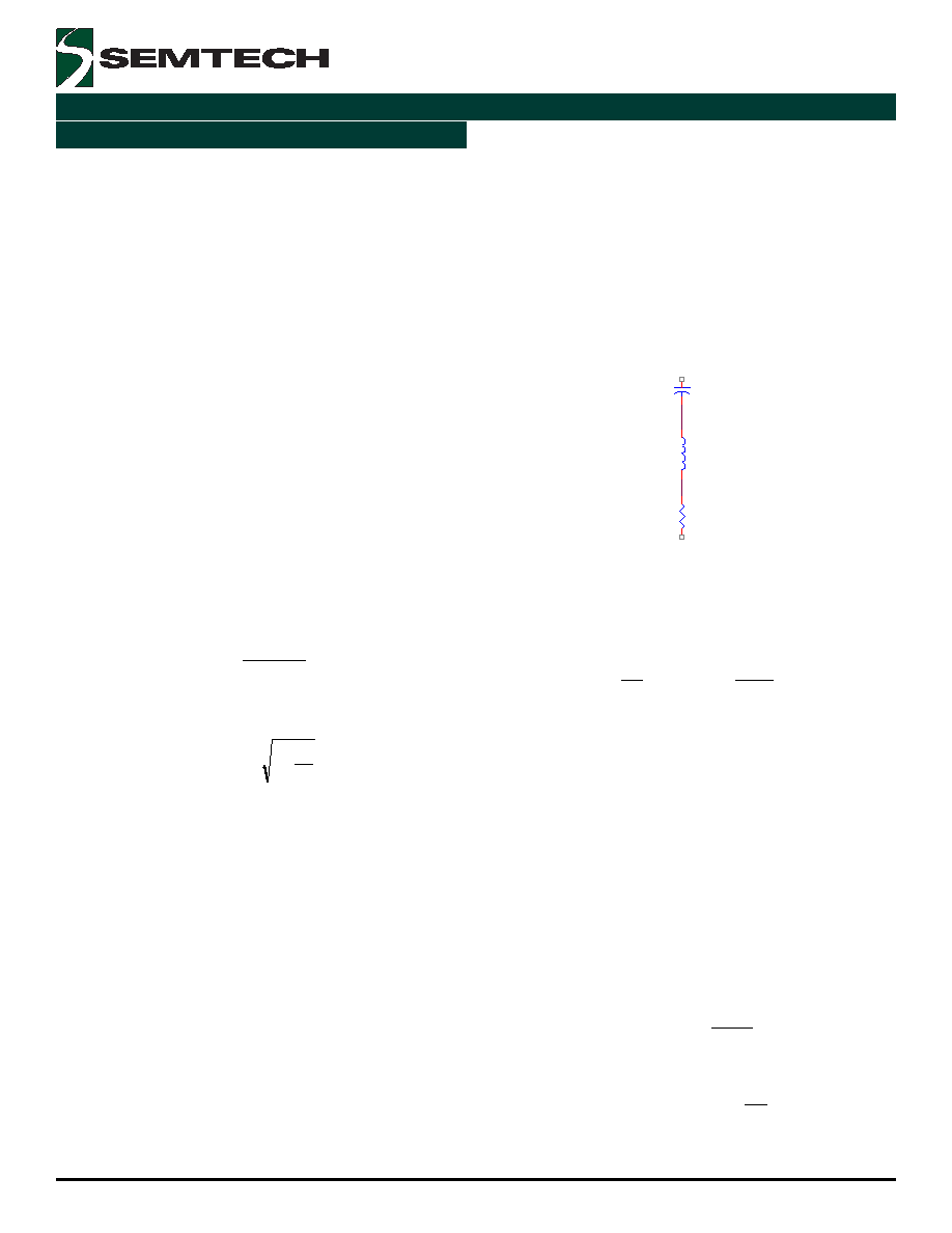 11 2005 Semtech Corp. www.semtech.com SC2453 POWER MANAGEMENT Applications Information (Cont.) There will not be enough modulation headroom if the on time is simply made equal to the minimum on time of the SC2453. For ease of control, we recommend the required pulse width to be at least 1.5 times the minimum on time. IIIIInductor (L) and Ripple Current nductor (L) and Ripple Current nductor (L) and Ripple Current nductor (L) and Ripple Current nductor (L) and Ripple Current Both step-down controllers in the SC2453 operate in synchronous continuous-conduction mode (CCM) regardless of the output load. The output inductor selection/design is based on the output DC and transient requirements. Both output current and voltage ripples are reduced with larger inductors but it takes longer to change the inductor current during load transients. Conversely smaller inductors results in lower DC copper losses but the AC core losses (flux swing) and the winding AC resistance losses are higher. A compromise is to choose the inductance such that peak-to-peak inductor ripple-current is 20% to 30% of the rated output load current. Assuming that the inductor current ripple (peak-to-peak) value is δ*I o, the inductance value will then be: s o o f I ) D 1 ( V L δ − = The peak current in the inductor becomes (1+ δ/2)*Io and the RMS current is: 12 1 I I 2 o rms , L δ + = The followings are to be considered when choosing inductors. a) Inductor core material: For high efficiency applications above 350KHz, ferrite, Kool-Mu and polypermalloy materials should be used. Low-cost powdered iron cores can be used for cost sensitive-applications below 350KHz but with attendant higher core losses. b) Select inductance value: Sometimes the calculated inductance value is not available off-the-shelf. The designer can choose the adjacent (larger) standard inductance value. The inductance varies with temperature and DC current. It is a good engineering practice to re-evaluate the resultant current ripple at the rated DC output current. c) Current rating: The saturation current of the inductor should be at least 1.5 times of the peak inductor current under all conditions. Output Capacitor (C Output Capacitor (C Output Capacitor (C Output Capacitor (C Output Capacitor (C ooooo) and V ) and V ) and V ) and V ) and V out out out out out Ripple Ripple Ripple Ripple Ripple The output capacitor provides output current filtering in steady state and serves as a reservoir during load transient. The output capacitor can be modeled as an ideal capacitor in series with its parasitic ESR (R esr) and ESL (L esl) (Figure 1). Co Lesl Resr Figure 1. An equivalent circuit of C o. If the current through the branch is i b(t), the voltage across the terminals will then be: ) t ( i R dt ) t ( di L dt ) t ( i C 1 V ) t ( v b esr t 0 b esl b o o o + + + = ∫ This basic equation illustrates the effect of ESR, ESL and C o on the output voltage. The first term is the DC voltage across C o at time t=0. The second term is the voltage variation caused by the charge balance between the load and the converter output. The third term is voltage ripple due to ESL and the fourth term is the voltage ripple due to ESR. The total output voltage ripple is then a vector sum of the last three terms. Since the inductor current is a triangular waveform with peak-to-peak value δ*I o, the ripple-voltage caused by inductor current ripples is: s o o C f C 8 I v δ ≈ ∆ the ripple-voltage due to ESL is: D I f L v o s esl ESL δ = ∆ and the ESR ripple-voltage is: |
|
|
Link URL |
| Does ALLDATASHEET help your business so far? [ DONATE ] |
About Alldatasheet | Advertisement | Contact us | Privacy Policy | Link to Datasheet | Link Exchange | Manufacturer List All Rights Reserved©Alldatasheet.com |
| Russian : Alldatasheetru.com | Korean : Alldatasheet.co.kr | Spanish : Alldatasheet.es | French : Alldatasheet.fr | Italian : Alldatasheetit.com Portuguese : Alldatasheetpt.com | Polish : Alldatasheet.pl | Vietnamese : Alldatasheet.vn Indian : Alldatasheet.in | Mexican : Alldatasheet.com.mx | British : Alldatasheet.co.uk | New Zealand : Alldatasheet.co.nz |
|
Family Site : ic2ic.com |
icmetro.com |
 British ▼
 English
 Chinese
 German
 Japanese
 Russian
 Korean
 Spanish
 French
 Italian
 Portuguese
 Polish
 Vietnamese
 Indian
 Mexican
 British
 New Zealand