|
Electronic Components Datasheet Search |
|
|
Electronic Components Datasheet Search |
|
H8SX/1663 Datasheet(PDF) 912 Page - Renesas Technology Corp |
|
|
|||||||||||||||||||||||||||||
H8SX/1663 Datasheet(HTML) 912 Page - Renesas Technology Corp |
|
|
912 / 1158 page 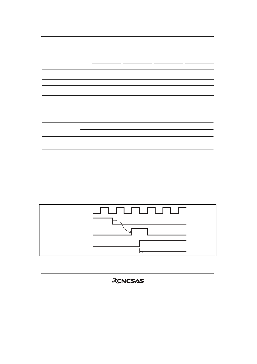 Section 18 A/D Converter Rev.1.00 Jun. 07, 2006 Page 860 of 1102 REJ09B0294-0100 Table 18.3 A/D Conversion Characteristics (Single Mode) CKS1 = 0 CKS1 = 1 CKS0 = 0 CKS0 = 1 CKS0 = 0 CKS0 = 1 Item Symbol Min. Typ. Max. Min. Typ. Max. Min. Typ. Max. Min. Typ. Max. A/D conversion start delay time t D 18 33 10 17 6 9 4 5 Input sampling time t SPL 127 63 31 15 A/D conversion time t CONV 515 530 259 266 131 134 67 68 Note: Values in the table are the number of states. Table 18.4 A/D Conversion Characteristics (Scan Mode) CKS1 CKS0 Conversion Time (Number of States) 0 512 (Fixed) 0 1 256 (Fixed) 0 128 (Fixed) 1 1 64 (Fixed) 18.4.4 External Trigger Input Timing A/D conversion can be externally triggered. When the TRGS1 and TRGS0 bits are set to B'11 in ADCR, an external trigger is input from the ADTRG0 pin. A/D conversion starts when the ADST bit in ADCSR is set to 1 on the falling edge of the ADTRG0 pin. Other operations, in both single and scan modes, are the same as when the ADST bit has been set to 1 by software. Figure 18.5 shows the timing. P φ ADTRG0 Internal trigger signal ADST A/D conversion Figure 18.5 External Trigger Input Timing |
|
Link URL |
| Does ALLDATASHEET help your business so far? [ DONATE ] |
About Alldatasheet | Advertisement | Contact us | Privacy Policy | Link to Datasheet | Link Exchange | Manufacturer List All Rights Reserved©Alldatasheet.com |
| Russian : Alldatasheetru.com | Korean : Alldatasheet.co.kr | Spanish : Alldatasheet.es | French : Alldatasheet.fr | Italian : Alldatasheetit.com Portuguese : Alldatasheetpt.com | Polish : Alldatasheet.pl | Vietnamese : Alldatasheet.vn Indian : Alldatasheet.in | Mexican : Alldatasheet.com.mx | British : Alldatasheet.co.uk | New Zealand : Alldatasheet.co.nz |
|
Family Site : ic2ic.com |
icmetro.com |
 British ▼
 English
 Chinese
 German
 Japanese
 Russian
 Korean
 Spanish
 French
 Italian
 Portuguese
 Polish
 Vietnamese
 Indian
 Mexican
 British
 New Zealand