 |
Electronic Components Datasheet Search |
|
|
Electronic Components Datasheet Search |
|
H8SX/1663R Datasheet(PDF) 977 Page - Renesas Technology Corp |
|
|
|||||||||||||||||||||||||||||
H8SX/1663R Datasheet(HTML) 977 Page - Renesas Technology Corp |
|
|
977 / 1504 page 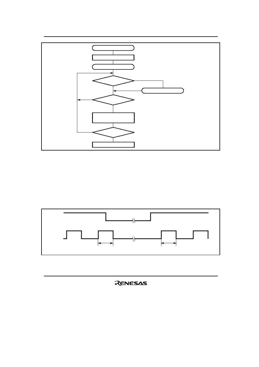 Section 19 Serial Communication Interface (SCI, IrDA, CRC) Rev. 2.00 Sep. 24, 2008 Page 945 of 1468 REJ09B0412-0200 Initialization Read data from RDR and clear RDRF flag in SSR to 0 Clear RE bit in SCR to 0 Start reception Start Error processing No No No Yes Yes ORER = 0 and PER = 0? RDRF = 1? All data received? Yes Figure 19.33 Sample Reception Flowchart 19.7.8 Clock Output Control (Only SCI_0, 1, 2, and 4) Clock output can be fixed using the CKE1 and CKE0 bits in SCR when the GM bit in SMR is set to 1. Specifically, the minimum width of a clock pulse can be specified. Figure 19.34 shows an example of clock output fixing timing when the CKE0 bit is controlled with GM = 1 and CKE1 = 0. Given pulse width SCK CKE0 Given pulse width Figure 19.34 Clock Output Fixing Timing |
|
Link URL |
| Does ALLDATASHEET help your business so far? [ DONATE ] |
About Alldatasheet | Advertisement | Contact us | Privacy Policy | Link to Datasheet | Link Exchange | Manufacturer List All Rights Reserved©Alldatasheet.com |
| Russian : Alldatasheetru.com | Korean : Alldatasheet.co.kr | Spanish : Alldatasheet.es | French : Alldatasheet.fr | Italian : Alldatasheetit.com Portuguese : Alldatasheetpt.com | Polish : Alldatasheet.pl | Vietnamese : Alldatasheet.vn Indian : Alldatasheet.in | Mexican : Alldatasheet.com.mx | British : Alldatasheet.co.uk | New Zealand : Alldatasheet.co.nz |
|
Family Site : ic2ic.com |
icmetro.com |
 British ▼
 English
 Chinese
 German
 Japanese
 Russian
 Korean
 Spanish
 French
 Italian
 Portuguese
 Polish
 Vietnamese
 Indian
 Mexican
 British
 New Zealand


