|
Electronic Components Datasheet Search |
|
|
Electronic Components Datasheet Search |
|
AS29F040CW-120/Q Datasheet(PDF) 5 Page - Austin Semiconductor |
|
|
|||||||||||||||||||||||||||||
AS29F040CW-120/Q Datasheet(HTML) 5 Page - Austin Semiconductor |
|
|
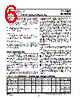
5 / 27 page  FLASH FLASH FLASH FLASH FLASH AS29F040 AustinSemiconductor,Inc.reservestherighttochangeproductsorspecificationswithoutnotice. 5 AS29F040 Rev. 2.2 09/07 Austin Semiconductor, Inc. Standby Mode When the system is not reading or writing to the device, it can place the device in the standby mode. In this mode, current consumption is greatly reduced, and the outputs are placed in the high impedance state, independent of the OE\ input. The device enters the CMOS standby mode when the CE\ pin is held at V CC ± 0.5V. (Note that this is a more restricted voltage range than V IH .) The device enters the TTL standby mode when CE\ is held at V IH. The device requires the standard access time (t CE ) before it is ready to read data. If the device is deselected during erasure or programming, the device draws active current until the operation is completed. I CC3 in the DC Characteristics table represents the standby current specification. Output Disable Mode When the OE\ input is at V IH , output from the device is disabled. The output pins are placed in the high impedance state. Autoselect Mode The autoselect mode provides manufacturer and device identification, and sector protection verification, through identifier codes output on DQ7 - DQ0. This mode is primarily intended for programming equipment to automatically match a device to be programmed with its corresponding programming algorithm. However, the autoselect codes can also be accessed in-system through the command register. When using programming equipment, the autoselect mode requires V ID (11.5V to 12.5 V) on address pin A9. Address pins A6, A1, and A0 must be as shown in the Autoselect Codes (High Voltage Method) table. In addition, when verifying sector protection, the sector address must appear on the appropriate highest order address bits. Refer to the corresponding Sector Address Tables. The Command TABLE 2: SECTOR ADDRESSES TABLE NOTE: All sectors are 64 Kbytes in size. Definitions table shows the remaining address bits that are don’t care. When all necessary bits have been set as required, the programming equipment may then read the corresponding identifier code on DQ7 - DQ0 To access the autoselect codes in-system, the host system can issue the autoselect command via the command register, as shown in the Command Definitions table. This method does not require V ID . See “Command Definitions” for details on using the autoselect mode. Sector Protection/Unprotection The hardware sector protection feature disables both program and erase operations in any sector. The hardware sector unprotection feature re-enables both program and erase operations in previously protected sectors. Sector protection/unprotection must be implemented using programming equipment. The procedure requires a high voltage (V ID ) on address pin A9 and the control pins. The device is shipped with all sectors unprotected. It is possible to determine whether a sector is protected or unprotected. See “Autoselect Mode” for details. Hardware Data Protection The command sequence requirement of unlock cycles for programming or erasing provides data protection against inadvertent writes (refer to the Command Definitions table). In addition, the following hardware data protection measures prevent accidental erasure or programming, which might otherwise be caused by spurious system level signals during V CC power-up and power-down transitions, or from system noise. Low V CC Write Inhibit When V CC is less than V LKO , the device does not accept any write cycles. This protects data during V CC power-up and SECTOR A18 A17 A16 ADDRESS RANGE SA0 0 0 0 00000h - 0FFFFh SA1 0 0 1 10000h - 1FFFFh SA2 0 1 0 20000h - 2FFFFh SA3 0 1 1 30000h - 3FFFFh SA4 1 0 0 40000h - 4FFFFh SA5 1 0 1 50000h - 5FFFFh SA6 1 1 0 60000h - 6FFFFh SA7 1 1 1 70000h - 7FFFFh |
|
Link URL |
| Does ALLDATASHEET help your business so far? [ DONATE ] |
About Alldatasheet | Advertisement | Contact us | Privacy Policy | Link to Datasheet | Link Exchange | Manufacturer List All Rights Reserved©Alldatasheet.com |
| Russian : Alldatasheetru.com | Korean : Alldatasheet.co.kr | Spanish : Alldatasheet.es | French : Alldatasheet.fr | Italian : Alldatasheetit.com Portuguese : Alldatasheetpt.com | Polish : Alldatasheet.pl | Vietnamese : Alldatasheet.vn Indian : Alldatasheet.in | Mexican : Alldatasheet.com.mx | British : Alldatasheet.co.uk | New Zealand : Alldatasheet.co.nz |
|
Family Site : ic2ic.com |
icmetro.com |
 British ▼
 English
 Chinese
 German
 Japanese
 Russian
 Korean
 Spanish
 French
 Italian
 Portuguese
 Polish
 Vietnamese
 Indian
 Mexican
 British
 New Zealand