|
Electronic Components Datasheet Search |
|
|
Electronic Components Datasheet Search |
|
ADP1046ACPZ-R7 Datasheet(PDF) 73 Page - Analog Devices |
|
|
|||||||||||||||||||||||||||||
ADP1046ACPZ-R7 Datasheet(HTML) 73 Page - Analog Devices |
|
|
73 / 96 page 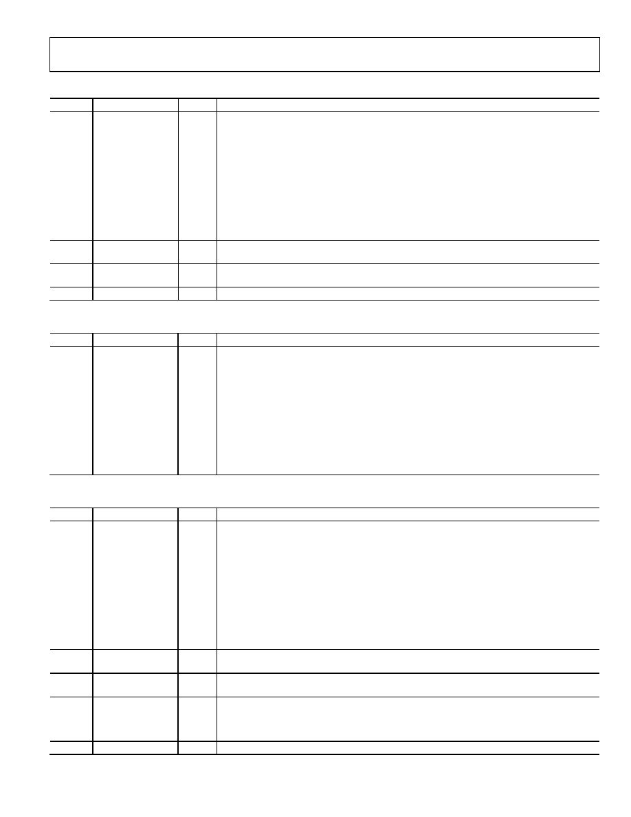 Data Sheet ADP1046 Rev. 0 | Page 73 of 96 Table 90. Register 0x5A—OUTAUX Rising Edge Setting (OUTAUX Pin) Bits Bit Name R/W Description [7:4] t13 R/W These bits contain the four LSBs of the 12-bit t13 time. This value is always used with the eight bits of Register 0x59, which contains the eight MSBs of the t13 time. Each LSB corresponds to 5 ns resolution. The entire switching period is divided into 40 ns time steps. If the t_rise and t_fall of a PWM edge occur within the same 40 ns time step, the PWM output is 0 V. If the t_rise and t_fall occur in different 40 ns time steps, the PWM output is set to the programmed value. The absolute maximum pulse width is tPERIOD − 5 ns. Depending on the switching frequency and the OUTAUX frequency, there is a constant lag/lead time between this edge and the other edges (t1 to t12); there- fore, OUTAUX is not synchronized to the other PWM outputs but can be made synchronous by adjusting the delay accordingly. If either the OUTAUX switching frequency (Register 0x3F) or the PWM switching frequency (Register 0x40) is changed after edge adjustment, the synchronization between OUTAUX and the PWM edges is no longer maintained. The OUTAUX delay must be adjusted again to synchronize the edges to the PWM edges for the new set of switching frequencies. 3 Modulate enable R/W 1 = PWM modulation acts on the t13 edge. 0 = no PWM modulation of the t13 edge. 2 t13 sign R/W 1 = negative sign. Increase of PWM modulation moves t13 right. 0 = positive sign. Increase of PWM modulation moves t13 left. [1:0] Reserved R/W Reserved. Table 91. Register 0x5B—OUTAUX Falling Edge Timing (OUTAUX Pin) Bits Bit Name R/W Description [7:0] t14 R/W This register contains the eight MSBs of the 12-bit t14 time. This value is always used with the top four bits of Register 0x5C, which contains the four LSBs of the t14 time. Each LSB corresponds to 5 ns resolution. The entire switching period is divided into 40 ns time steps. If the t_rise and t_fall of a PWM edge occur within the same 40 ns time step, the PWM output is 0 V. If the t_rise and t_fall occur in different 40 ns time steps, the PWM output is set to the programmed value. The absolute maximum pulse width is tPERIOD − 5 ns. Depending on the switching frequency and the OUTAUX frequency, there is a constant lag/lead time between this edge and the other edges (t1 to t12); there- fore, OUTAUX is not synchronized to the other PWM outputs but can be made synchronous by adjusting the delay accordingly. If either the OUTAUX switching frequency (Register 0x3F) or the PWM switching frequency (Register 0x40) is changed after edge adjustment, the synchronization between OUTAUX and the PWM edges is no longer maintained. The OUTAUX delay must be adjusted again to synchronize the edges to the PWM edges for the new set of switching frequencies. Table 92. Register 0x5C—OUTAUX Falling Edge Setting (OUTAUX Pin) Bits Bit Name R/W Description [7:4] t14 R/W These bits contain the four LSBs of the 12-bit t14 time. This value is always used with the eight bits of Register 0x5B, which contains the eight MSBs of the t14 time. Each LSB corresponds to 5 ns resolution. The entire switching period is divided into 40 ns time steps. If the t_rise and t_fall of a PWM edge occur within the same 40 ns time step, the PWM output is 0 V. If the t_rise and t_fall occur in different 40 ns time steps, the PWM output is set to the programmed value. The absolute maximum pulse width is tPERIOD − 5 ns. Depending on the switching frequency and the OUTAUX frequency, there is a constant lag/lead time between this edge and the other edges (t1 to t12); there- fore, OUTAUX is not synchronized to the other PWM outputs but can be made synchronous by adjusting the delay accordingly. If either the OUTAUX switching frequency (Register 0x3F) or the PWM switching frequency (Register 0x40) is changed after edge adjustment, the synchronization between OUTAUX and the PWM edges is no longer maintained. The OUTAUX delay must be adjusted again to synchronize the edges to the PWM edges for the new set of switching frequencies. 3 Modulate enable R/W 1 = PWM modulation acts on the t14 edge. 0 = no PWM modulation of the t14 edge. 2 t14 sign R/W 1 = negative sign. Increase of PWM modulation moves t14 right. 0 = positive sign. Increase of PWM modulation moves t14 left. 1 Regulate with OUTAUX R/W 1 = control loop PWM modulation is regulated by OUTAUX. When this bit is set, the CS1 blanking signal is synchronized with OUTAUX. 0 = control loop PWM modulation is regulated by OUTA, OUTB, OUTC, OUTD, SR1, and SR2 (normal mode). 0 Reserved R/W Reserved. Set this bit to 0 for normal operation. |
|
Link URL |
| Does ALLDATASHEET help your business so far? [ DONATE ] |
About Alldatasheet | Advertisement | Contact us | Privacy Policy | Link to Datasheet | Link Exchange | Manufacturer List All Rights Reserved©Alldatasheet.com |
| Russian : Alldatasheetru.com | Korean : Alldatasheet.co.kr | Spanish : Alldatasheet.es | French : Alldatasheet.fr | Italian : Alldatasheetit.com Portuguese : Alldatasheetpt.com | Polish : Alldatasheet.pl | Vietnamese : Alldatasheet.vn Indian : Alldatasheet.in | Mexican : Alldatasheet.com.mx | British : Alldatasheet.co.uk | New Zealand : Alldatasheet.co.nz |
|
Family Site : ic2ic.com |
icmetro.com |
 British ▼
 English
 Chinese
 German
 Japanese
 Russian
 Korean
 Spanish
 French
 Italian
 Portuguese
 Polish
 Vietnamese
 Indian
 Mexican
 British
 New Zealand