|
Electronic Components Datasheet Search |
|
|
Electronic Components Datasheet Search |
|
AD9739-R2-EBZ Datasheet(PDF) 31 Page - Analog Devices |
|
|
|||||||||||||||||||||||||||||
AD9739-R2-EBZ Datasheet(HTML) 31 Page - Analog Devices |
|
|
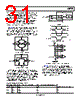
31 / 48 page 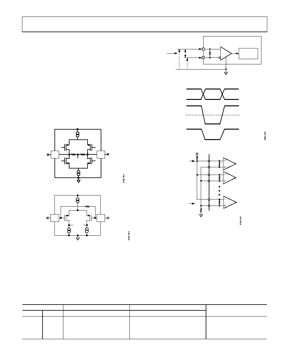 Data Sheet AD9739 Rev. B | Page 31 of 48 LVDS INPUTS (NO FAIL-SAFE) VP LVDS RECEIVER GND 100Ω VN VP,N VCOM = (VP + VN)/2 LOGIC BIT EQUIVALENT VP VN VP VN EXAMPLE 1.4V 1.0V 0.4V –0.4V 0V LOGIC 1 LOGIC 0 Rotating the CLKDIVPH phase provides a means of adjusting the delay in course steps of fDAC/4. For example, in the 800 MSPS and 1600 MSPS cases described above, rotating the CLKDIVPH setting by 1 corresponds to a delay shift of 5 ns and 2.5 ns, respectively. By adding an additional step in the SPI initialization routine for the data receiver controller, it becomes possible to increase the effective range of the delay line to ensure a DCI_DEL value that falls within a reasonable guard band. LVDS Driver and Receiver Input The AD9739 features a LVDS-compatible driver and receivers. The LVDS driver output used for the DCO and SYNC_OUT signal includes an equivalent 200 Ω source resistor that limits its nominal output voltage swing to ±200 mV when driving a 100 Ω load. The DCO output driver can be powered down via Register 0x01, Bit 5. An equivalent circuit is shown in Figure 44 DCO_N VSS VDD33 DCO_P V+ V+ V– V– 100Ω VCM 100Ω ESD ESD Figure 46. LVDS Data Input Levels 100Ω 100Ω 100Ω VDD33 = 3.3V LVDS_1 LVDS_N LVDS_2 VP = 1.4V R1 R2 VP = 1.4V R1 = 4.75 × 100/N R2 = 2.50 × 100/N Figure 44. Equivalent LVDS Output VSS VDD33 DCI_P DBx[13:0]P DCI_N DBx[13:0]N 100Ω ESD ESD Figure 45. Equivalent LVDS Input The LVDS receivers include 100 Ω termination resistors, as shown in Figure 45. These receivers meet the IEEE-1596.3-1996 reduced swing specification (with the exception of input hysteresis, which cannot be guaranteed over all process corners). Figure 46 and Figure 47 show an example of nominal LVDS voltage levels seen at the input of the differential receiver with resulting common- mode voltage and equivalent logic level. The LVDS receivers can be powered down via Register 0x01, Bit 4. Figure 47. Resistor Network to Bias Unused LVDS Data Inputs The AD9739 LVDS inputs do not include fail-safe capability. Any unused data input pins should be biased with an external network or static driver. Figure 47 shows an external biasing network that can be used to place unused data bits into a known state. The resistor values for R1 and R2 are selected to establish a VP and VN of 1.4 V and 1.0 V, respectively, depending on the number of unused digital inputs, N. Table 27. Example of LVDS Input Levels Applied Voltages Resulting Differential Voltage Resulting Common-Model Voltage VP (V) VN (V) VP, N VCOM Logic Bit Binary Equivalent 1.4 1.0 +0.4 V 1.2 V 1 1.0 1.4 −0.4 V 1.2 V 0 1.0 0.8 +200 mV 900 mV 1 0.8 1.0 −200 mV 900 mV 0 |
|
Link URL |
| Does ALLDATASHEET help your business so far? [ DONATE ] |
About Alldatasheet | Advertisement | Contact us | Privacy Policy | Link to Datasheet | Link Exchange | Manufacturer List All Rights Reserved©Alldatasheet.com |
| Russian : Alldatasheetru.com | Korean : Alldatasheet.co.kr | Spanish : Alldatasheet.es | French : Alldatasheet.fr | Italian : Alldatasheetit.com Portuguese : Alldatasheetpt.com | Polish : Alldatasheet.pl | Vietnamese : Alldatasheet.vn Indian : Alldatasheet.in | Mexican : Alldatasheet.com.mx | British : Alldatasheet.co.uk | New Zealand : Alldatasheet.co.nz |
|
Family Site : ic2ic.com |
icmetro.com |
 British ▼
 English
 Chinese
 German
 Japanese
 Russian
 Korean
 Spanish
 French
 Italian
 Portuguese
 Polish
 Vietnamese
 Indian
 Mexican
 British
 New Zealand