|
Electronic Components Datasheet Search |
|
|
Electronic Components Datasheet Search |
|
AT86RF211DAI-R Datasheet(PDF) 32 Page - ATMEL Corporation |
|
|
|||||||||||||||||||||||||||||
AT86RF211DAI-R Datasheet(HTML) 32 Page - ATMEL Corporation |
|
|
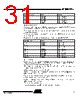
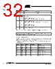
32 / 48 page 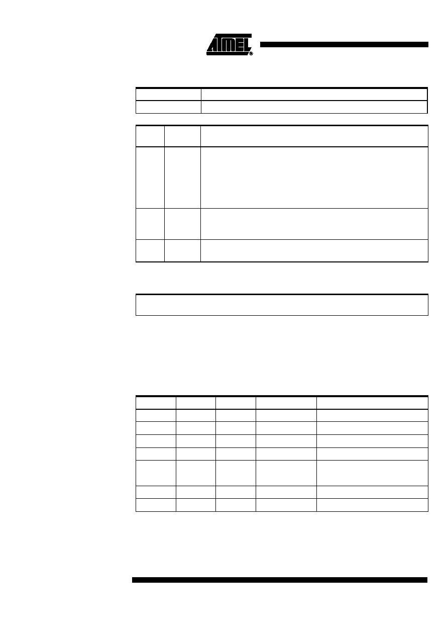 32 AT86RF211 1942C–WIRE–06/02 Frequency Registers Note: 1. F0, F1, F2 and F3 registers must be programmed before using the device. • Frequency Registers Selection The FSK modulation is completely integrated. Two registers have to be programmed (default F0 and F1) to allow "0" and "1" transmission. The frequency register selection depends on the control register programming and on the DATAMSG pin: Table 9. Frequency Registers Name F0, F1, F2, F3 nbit 31-0 Name Number of bits Comments F0 32 Frequency code value F0 default register in TX mode ("0" code in FSK modulation). F1 32 Frequency code value F1 default register in TX mode ("1" code frequency in FSK modulation). F2 32 Frequency code value F2 default register in RX mode. F3 32 Frequency code value F3 There is no simple relationship between frequency registers and the exact frequency. Atmel provides a tool to program them on a production bench. RXTX RXFS TXFS DATAMSG Mode 0 00 X X Receive LO is F0 0 01 X X Receive LO is F1 0 10 X X Receive LO is F2 0 11 X X Receive LO is F3 1 XX 0 0 Transmit "0" on F0 1 XX 0 1 Transmit "1" on F1 1 XX 1 0 Transmit "0" on F2 1 XX 1 1 Transmit "1" on F3 |
|
Link URL |
| Does ALLDATASHEET help your business so far? [ DONATE ] |
About Alldatasheet | Advertisement | Contact us | Privacy Policy | Link to Datasheet | Link Exchange | Manufacturer List All Rights Reserved©Alldatasheet.com |
| Russian : Alldatasheetru.com | Korean : Alldatasheet.co.kr | Spanish : Alldatasheet.es | French : Alldatasheet.fr | Italian : Alldatasheetit.com Portuguese : Alldatasheetpt.com | Polish : Alldatasheet.pl | Vietnamese : Alldatasheet.vn Indian : Alldatasheet.in | Mexican : Alldatasheet.com.mx | British : Alldatasheet.co.uk | New Zealand : Alldatasheet.co.nz |
|
Family Site : ic2ic.com |
icmetro.com |
 British ▼
 English
 Chinese
 German
 Japanese
 Russian
 Korean
 Spanish
 French
 Italian
 Portuguese
 Polish
 Vietnamese
 Indian
 Mexican
 British
 New Zealand