|
Electronic Components Datasheet Search |
|
|
Electronic Components Datasheet Search |
|
AS7C316096C Datasheet(PDF) 8 Page - Alliance Semiconductor Corporation |
|
|
|||||||||||||||||||||||||||||
AS7C316096C Datasheet(HTML) 8 Page - Alliance Semiconductor Corporation |
|
|
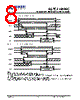
8 / 12 page  AS7C316096C Rev. 1.0 2048K X 8 BIT HIGH SPEED CMOS SRAM Confidential 7 Rev 1.0 / May 2014 WRITE CYCLE 1 (WE# Controlled) (1,2,3,5,6) Dout Din Data Valid tDW tDH (4) High-Z tWHZ WE# tWP tCW CE# tWR tAS tAW Address tWC (4) TOW WRITE CYCLE 2 (CE# Controlled) (1,2,5,6) Dout Din Data Valid tDW tDH (4) High-Z tWHZ WE# tWP tCW CE# tWR tAS tAW Address tWC Notes : 1.WE#,CE#, LB#, UB# must be high during all address transitions. 2.A write occurs during the overlap of a low CE#, low WE#, LB# or UB# = low. 3.During a WE# controlled write cycle with OE# low, tWP must be greater than tWHZ + tDW to allow the drivers to turn off and data to be placed on the bus. 4.During this period, I/O pins are in the output state, and input signals must not be applied. 5.If the CE#, LB#, UB# low transition occurs simultaneously with or after WE# low transition, the outputs remain in a high impedance state. 6.tOW and tWHZ are specified with CL = 5pF. Transition is measured ±500mV from steady state. |
|
|
Link URL |
| Does ALLDATASHEET help your business so far? [ DONATE ] |
About Alldatasheet | Advertisement | Contact us | Privacy Policy | Link to Datasheet | Link Exchange | Manufacturer List All Rights Reserved©Alldatasheet.com |
| Russian : Alldatasheetru.com | Korean : Alldatasheet.co.kr | Spanish : Alldatasheet.es | French : Alldatasheet.fr | Italian : Alldatasheetit.com Portuguese : Alldatasheetpt.com | Polish : Alldatasheet.pl | Vietnamese : Alldatasheet.vn Indian : Alldatasheet.in | Mexican : Alldatasheet.com.mx | British : Alldatasheet.co.uk | New Zealand : Alldatasheet.co.nz |
|
Family Site : ic2ic.com |
icmetro.com |
 British ▼
 English
 Chinese
 German
 Japanese
 Russian
 Korean
 Spanish
 French
 Italian
 Portuguese
 Polish
 Vietnamese
 Indian
 Mexican
 British
 New Zealand