 |
Electronic Components Datasheet Search |
|
|
Electronic Components Datasheet Search |
|
A4923GETTR-R Datasheet(PDF) 7 Page - Allegro MicroSystems |
|
|
|||||||||||||||||||||||||||||
A4923GETTR-R Datasheet(HTML) 7 Page - Allegro MicroSystems |
|
|
7 / 11 page 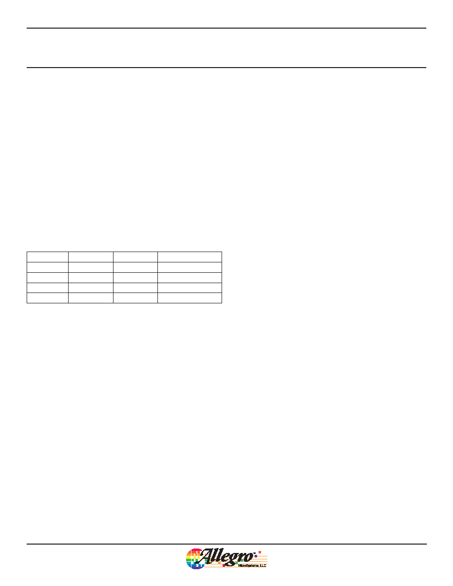 3-Phase Sinusoidal Motor Controller A4923 6 Allegro MicroSystems, LLC 115 Northeast Cutoff Worcester, Massachusetts 01615-0036 U.S.A. 1.508.853.5000; www.allegromicro.com Functional Description STARTn The STARTn terminal is the active-low start/stop logic input. (low = start, high = all gate drive outputs off). Internally pulled up to VREG3.3. BRAKE The BRAKE terminal is the active-high logic input to turn on all low-side MOSFETs. The STARTn terminal must be active (low) to enable brake. Internally pulled up to VREG3.3 DIR The DIR terminal is the logic input to control the motor’s direc- tion. A logic high = FWD and a logic low = REV. Internally pulled up to VREG3.3. Table 1: STARTn BRAKEn Fault Function H X L All gate outputs low L L L Run L H L Brake X X H All gate outputs low FGO The FGO terminal is an open-drain logic output which toggles state each hall transition. TEST1, TEST2 The TEST1 and TEST2 terminals are for ATE testing and can be left open or tied to GND. Current Limit Over-current is controlled by an internal fixed off-time PWM control circuit. At the trip point, the sense comparator turns off the enabled low-side driver, turns on the corresponding high side driver, and the motor current recirculates through the high-side drivers. ITRIP = 240 mV / RSENSE Hall Inputs Unique circuitry incorporates hysteresis which toggles polarity with the hall input slope direction. This allows the hall com- parators to operate with very small offsets and results in highly symmetrical comparator outputs. A digital filter on the hall inputs minimizes sensitivity to noise. VPOS A 0.1 μF capacitor is required between this terminal and GND to stabilize the internal 3.3 V regulator VREG A 0.1 μF capacitor is required between this terminal and GND to stabilize the low-side gate supply. Charge Pump Terminals CP1, CP2, and VCP generate a voltage above VBB that is used for the high-side gate supply. A 0.1 μF capacitor is required between the CP1 and CP2 terminals, and between VCP and VBB. Fault A fault occurs when VBB, the charge pump, or HBIAS falls below the respective UVLO threshold, the device temperature rises above TJ, or the hall inputs indicate an invalid state (111 or 000). The outputs are disabled in the event of a fault. Faults are not latched, and the device resumes operation once the fault is cleared. |
|
|
Link URL |
| Does ALLDATASHEET help your business so far? [ DONATE ] |
About Alldatasheet | Advertisement | Contact us | Privacy Policy | Link to Datasheet | Link Exchange | Manufacturer List All Rights Reserved©Alldatasheet.com |
| Russian : Alldatasheetru.com | Korean : Alldatasheet.co.kr | Spanish : Alldatasheet.es | French : Alldatasheet.fr | Italian : Alldatasheetit.com Portuguese : Alldatasheetpt.com | Polish : Alldatasheet.pl | Vietnamese : Alldatasheet.vn Indian : Alldatasheet.in | Mexican : Alldatasheet.com.mx | British : Alldatasheet.co.uk | New Zealand : Alldatasheet.co.nz |
|
Family Site : ic2ic.com |
icmetro.com |
 British ▼
 English
 Chinese
 German
 Japanese
 Russian
 Korean
 Spanish
 French
 Italian
 Portuguese
 Polish
 Vietnamese
 Indian
 Mexican
 British
 New Zealand


