|
Electronic Components Datasheet Search |
|
|
Electronic Components Datasheet Search |
|
STPMS2 Datasheet(PDF) 24 Page - STMicroelectronics |
|
|
|||||||||||||||||||||||||||||
STPMS2 Datasheet(HTML) 24 Page - STMicroelectronics |
|
|
24 / 36 page 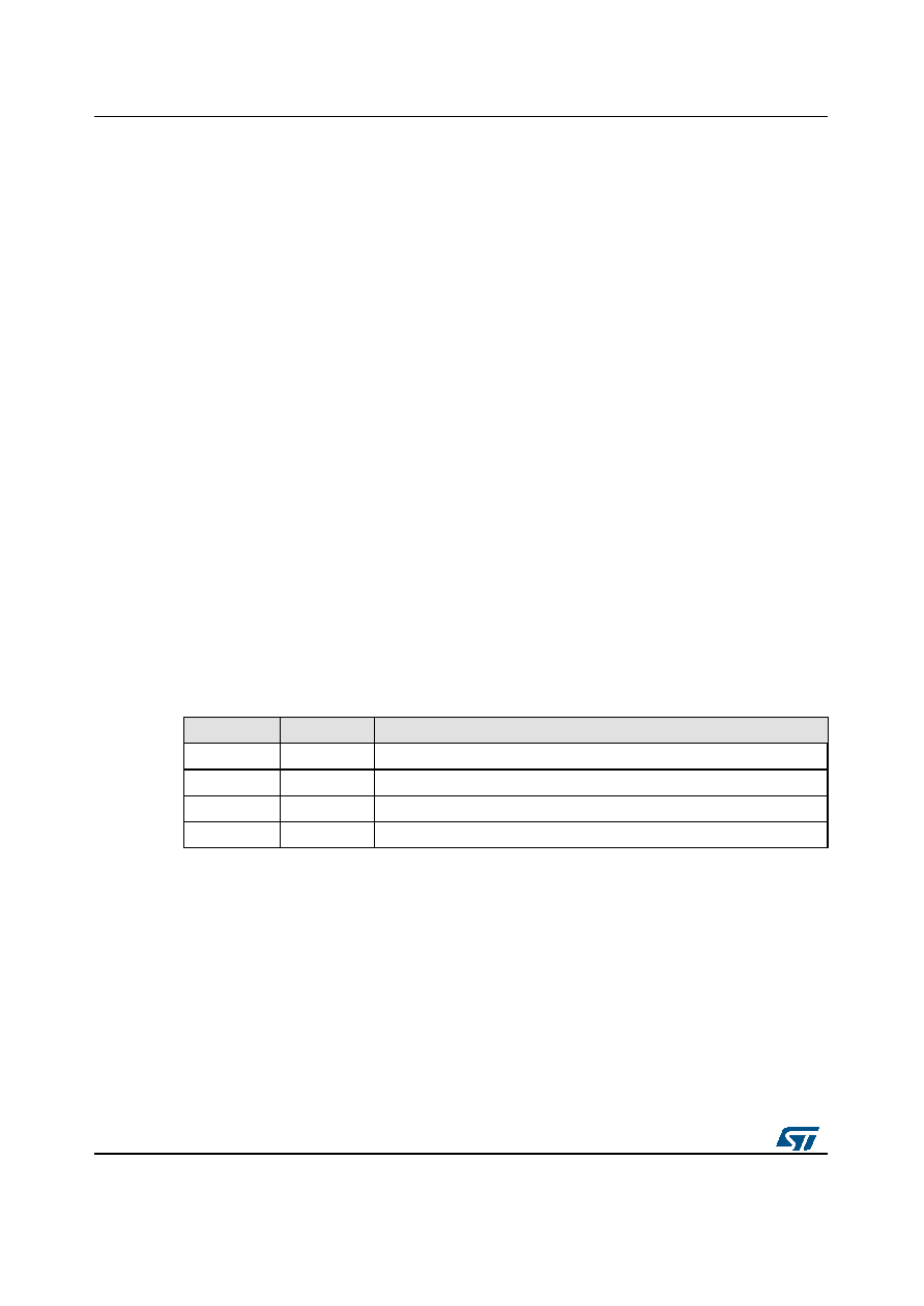 Theory of operation STPMS2 24/36 DocID16525 Rev 5 Synchro In synchro block the synchronization of sigma-delta input streams with strobe signals from analog part and clock signal is performed. Mux In the mux block signals, connected to output pins DAT and DATn, are selected. In hard mode, the output signals are selected by input pin MS2. In soft mode, the output signals are selected by 8 configuration bits. 9.4 Hard mode The STPMS2 works in hard mode when input pin MS3 is connected to GND or VCC, as described in Table 11. In hard mode, the STPMS2 has four digital input pins (MS0, MS1, MS2 and MS3) to configure the basic operating parameters: BIST DAC enable Temperature curve of reference voltage Current and voltage channel settings Output mode settings In this manner, 128 different combinations are available and they are controlled by MS0, MS1, MS2 and MS3 pins. MS0 sets the operating mode and amplifier gain selection as described in Table 8: "Precision mode and input amplifier gain selection" . MS0 = GND or CLK to select LPR (low precision); fCLK = 1 MHz is the typical input clock frequency and low power mode is selected. MS0 = NCLK or VCC to select HPR (high precision); fCLK = 2 or 4 MHz are the typical input clock frequencies and accuracy is enhanced. The relative gain of the current channel is selectable between 2 or 16, which defines the maximum differential voltage on the current channel to ± 300 mV or ± 37.5 mV, respectively. The voltage channel gain setting is fixed at 2, which defines the maximum differential voltage on the voltage channel inputs to ± 300 mV. Table 8: Precision mode and input amplifier gain selection MS0 Mode Description GND 0 LPR, amplifier GAIN selection g3 = 16 CLK 1 LPR, amplifier GAIN selection g0 = 2 NCLK 2 HPR, amplifier GAIN selection g0 = 2 VCC 3 HPR, amplifier GAIN selection g3 = 16 MS1 defines the temperature compensation (TC) curve of the internal voltage reference of the STPMS2, as described in Table 9: "TC of the bandgap reference" (characterized by application). The temperature-compensated reference voltage generator produces VREF = 1.23 V. This generator is implemented as a bandgap generator, whose temperature compensation curve can be selected by MS1 configuration pin. |
|
Link URL |
| Does ALLDATASHEET help your business so far? [ DONATE ] |
About Alldatasheet | Advertisement | Contact us | Privacy Policy | Link to Datasheet | Link Exchange | Manufacturer List All Rights Reserved©Alldatasheet.com |
| Russian : Alldatasheetru.com | Korean : Alldatasheet.co.kr | Spanish : Alldatasheet.es | French : Alldatasheet.fr | Italian : Alldatasheetit.com Portuguese : Alldatasheetpt.com | Polish : Alldatasheet.pl | Vietnamese : Alldatasheet.vn Indian : Alldatasheet.in | Mexican : Alldatasheet.com.mx | British : Alldatasheet.co.uk | New Zealand : Alldatasheet.co.nz |
|
Family Site : ic2ic.com |
icmetro.com |
 British ▼
 English
 Chinese
 German
 Japanese
 Russian
 Korean
 Spanish
 French
 Italian
 Portuguese
 Polish
 Vietnamese
 Indian
 Mexican
 British
 New Zealand