 |
Electronic Components Datasheet Search |
|
|
Electronic Components Datasheet Search |
|
The question interval is too short.
Please try again in a few seconds.

Hello, Please ask a question about TLE6258-2 Datasheet
# Example questions:
➢ What is the maximum wake-up delay time (t_wake) at a junction temperature (tj) of 150°c?
➢ What are the bus load conditions used for testing dynamic characteristics (specifically, what values are given for c_bus and r_bus)?
➢ What is the typical value and maximum value for the bus recessive output voltage (v_bus,rec)?
| Part No. | TLE6258-2 |
| Manufacturer | INFINEON |
| Size | 204 Kbytes |
| Pages | 15 pages |
| Description | LIN Transceiver |


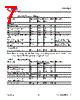
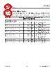
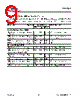


1. General Device Characteristics & Power Supply:
️· Operating Voltage: Not explicitly stated, but implied to be between 4.5V and 5.5V (VCC) and 6V to 27V (VS).
️· Temperature Range: -40°C to 125°C (for wake-up delay time) and -40°C to 150°C (for another wake-up delay time).
️· LIN Transceiver: Designed for Local Interconnect Network (LIN) communication.
2. Electrical Characteristics (Key Parameters)
| Parameter | Symbol | Min | Typ | Max | Units | Notes |
|---|---|---|---|---|---|---|
| Input/Output Voltages (Related to VS - Supply Voltage) | ||||||
| Dominant Output Voltage (Low) | V<sub>bus,dom</sub> | 0 | - | 1.2 | V | V<sub>CC</sub>=5V, V<sub>TxD</sub> = 0V. Range of VS=6-7.3V |
| Dominant Output Voltage (High) | V<sub>bus,dom</sub> | 0 | - | 2 | V | V<sub>CC</sub>=5V, V<sub>TxD</sub> =0V. Range of VS=7.3-27V |
| Recessive Output Voltage | V<sub>bus,rec</sub> | 0.9*V<sub>S</sub> | - | V<sub>S</sub> | V | V<sub>TxD</sub> = V<sub>CC</sub> |
| Wake-up Threshold Voltage | V<sub>wake</sub> | 0.4*V<sub>S</sub> | 0.5*V<sub>S</sub> | 0.6*V<sub>S</sub> | V | |
| Timing (Dynamic Characteristics - Critical for LIN Communication) | ||||||
| Propagation Delay TxD LOW to bus | t<sub>d(L),T</sub> | - | 1 | 3 | µs | V<sub>CC</sub> = 5 V |
| Propagation Delay TxD HIGH to bus | t<sub>d(H),T</sub> | - | 1 | 3 | µs | V<sub>CC</sub> = 5 V |
| Propagation Delay bus Dominant to RxD LOW | t<sub>d(L),R</sub> | - | 1 | 6 | µs | V<sub>CC</sub> = 5 V, C<sub>RxD</sub> = 20 pF |
| Propagation Delay bus Recessive to RxD High | t<sub>d(H),R</sub> | - | 1 | 6 | µs | V<sub>CC</sub> = 5 V, C<sub>RxD</sub> = 20 pF |
| Duty Cycle D1 | t<sub>duty1</sub> | 0.396 | - | - | µs | |
| Duty Cycle D2 | t<sub>duty2</sub> | - | - | 0.581 | µs | |
| Wake-up delay time | t<sub>wake</sub> | 30 | 100 | 150 | µs | T<sub>j</sub> < 125°C |
| Falling edge slew rate | S<sub>bus(L)</sub> | -3 | -2 | -1 | V/µs | 1) 60% > V > 40% Bus |
| Rising edge slew rate | S<sub>bus(H)</sub> | 1 | 1.5 | 3 | V/µs | |
| Short circuit current | I<sub>bus,sc</sub> | 40 | 100 | 150 | mA |
1. General Device Characteristics & Power Supply:
️· Operating Voltage: Not explicitly stated, but implied to be between 4.5V and 5.5V (VCC) and 6V to 27V (VS).
️· Temperature Range: -40°C to 125°C (for wake-up delay time) and -40°C to 150°C (for another wake-up delay time).
️· LIN Transceiver: Designed for Local Interconnect Network (LIN) communication.
2. Electrical Characteristics (Key Parameters)
| Parameter | Symbol | Min | Typ | Max | Units | Notes |
|---|---|---|---|---|---|---|
| Input/Output Voltages (Related to VS - Supply Voltage) | ||||||
| Dominant Output Voltage (Low) | V<sub>bus,dom</sub> | 0 | - | 1.2 | V | V<sub>CC</sub>=5V, V<sub>TxD</sub> = 0V. Range of VS=6-7.3V |
| Dominant Output Voltage (High) | V<sub>bus,dom</sub> | 0 | - | 2 | V | V<sub>CC</sub>=5V, V<sub>TxD</sub> =0V. Range of VS=7.3-27V |
| Recessive Output Voltage | V<sub>bus,rec</sub> | 0.9*V<sub>S</sub> | - | V<sub>S</sub> | V | V<sub>TxD</sub> = V<sub>CC</sub> |
| Wake-up Threshold Voltage | V<sub>wake</sub> | 0.4*V<sub>S</sub> | 0.5*V<sub>S</sub> | 0.6*V<sub>S</sub> | V | |
| Timing (Dynamic Characteristics - Critical for LIN Communication) | ||||||
| Propagation Delay TxD LOW to bus | t<sub>d(L),T</sub> | - | 1 | 3 | µs | V<sub>CC</sub> = 5 V |
| Propagation Delay TxD HIGH to bus | t<sub>d(H),T</sub> | - | 1 | 3 | µs | V<sub>CC</sub> = 5 V |
| Propagation Delay bus Dominant to RxD LOW | t<sub>d(L),R</sub> | - | 1 | 6 | µs | V<sub>CC</sub> = 5 V, C<sub>RxD</sub> = 20 pF |
| Propagation Delay bus Recessive to RxD High | t<sub>d(H),R</sub> | - | 1 | 6 | µs | V<sub>CC</sub> = 5 V, C<sub>RxD</sub> = 20 pF |
| Duty Cycle D1 | t<sub>duty1</sub> | 0.396 | - | - | µs | |
| Duty Cycle D2 | t<sub>duty2</sub> | - | - | 0.581 | µs | |
| Wake-up delay time | t<sub>wake</sub> | 30 | 100 | 150 | µs | T<sub>j</sub> < 125°C |
| Falling edge slew rate | S<sub>bus(L)</sub> | -3 | -2 | -1 | V/µs | 1) 60% > V > 40% Bus |
| Rising edge slew rate | S<sub>bus(H)</sub> | 1 | 1.5 | 3 | V/µs | |
| Short circuit current | I<sub>bus,sc</sub> | 40 | 100 | 150 | mA |
| Part No. | TLE6258-2 |
| Manufacturer | INFINEON |
| Size | 204 Kbytes |
| Pages | 15 pages |
| Description | LIN Transceiver |
| Does ALLDATASHEET help your business so far? [ DONATE ] |
About Alldatasheet | Advertisement | Contact us | Privacy Policy | Link to Datasheet | Link Exchange | Manufacturer List All Rights Reserved©Alldatasheet.com |
| Russian : Alldatasheetru.com | Korean : Alldatasheet.co.kr | Spanish : Alldatasheet.es | French : Alldatasheet.fr | Italian : Alldatasheetit.com Portuguese : Alldatasheetpt.com | Polish : Alldatasheet.pl | Vietnamese : Alldatasheet.vn Indian : Alldatasheet.in | Mexican : Alldatasheet.com.mx | British : Alldatasheet.co.uk | New Zealand : Alldatasheet.co.nz |
|
Family Site : ic2ic.com |
icmetro.com |
 British ▼
  English
 Chinese
 German
 Japanese
 Russian
 Korean
 Spanish
 French
 Italian
 Portuguese
 Polish
 Vietnamese
 Indian
 Mexican
 New Zealand