|
Electronic Components Datasheet Search |
|
|
Electronic Components Datasheet Search |
|
ZL30102 Datasheet(PDF) 9 Page - Zarlink Semiconductor Inc |
|
|
|||||||||||||||||||||||||||||
ZL30102 Datasheet(HTML) 9 Page - Zarlink Semiconductor Inc |
|
|
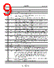
9 / 50 page  ZL30102 Data Sheet 9 Zarlink Semiconductor Inc. 2.2 Pin Description Pin # Name Description 1GND Ground. 0V 2VCORE Positive Supply Voltage. +1.8 VDC nominal 3LOCK Lock Indicator (Output). This output goes to a logic high when the PLL is frequency locked to the selected input reference. 4 HOLDOVER Holdover (Output). This output goes to a logic high whenever the PLL goes into holdover mode. 5 REF_FAIL0 Reference 0 Failure Indicator (Output). A logic high at this pin indicates that the REF0 reference frequency has exceeded the out-of-range limit set by the OOR_SEL pin or that it is exhibiting abrupt phase or frequency changes. 6 REF_FAIL1 Reference 1 Failure Indicator (Output). A logic high at this pin indicates that the REF1 reference frequency has exceeded the out-of-range limit set by the OOR_SEL pin or that it is exhibiting abrupt phase or frequency changes. 7 REF_FAIL2 Reference 2 Failure Indicator (Output). A logic high at this pin indicates that the REF2 reference frequency has exceeded the out-of-range limit set by the OOR_SEL pin or that it is exhibiting abrupt phase or frequency changes. 8TDO Test Serial Data Out (Output). JTAG serial data is output on this pin on the falling edge of TCK. This pin is held in high impedance state when JTAG scan is not enabled. 9TMS Test Mode Select (Input). JTAG signal that controls the state transitions of the TAP controller. This pin is internally pulled up to VDD. If this pin is not used then it should be left unconnected. 10 TRST Test Reset (Input). Asynchronously initializes the JTAG TAP controller by putting it in the Test-Logic-Reset state. This pin should be pulsed low on power-up to ensure that the device is in the normal functional state. This pin is internally pulled up to VDD. If this pin is not used then it should be connected to GND. 11 TCK Test Clock (Input): Provides the clock to the JTAG test logic. If this pin is not used then it should be pulled down to GND. 12 VCORE Positive Supply Voltage. +1.8 VDC nominal 13 GND Ground. 0V 14 AVCORE Positive Analog Supply Voltage. +1.8 VDC nominal 15 TDI Test Serial Data In (Input). JTAG serial test instructions and data are shifted in on this pin. This pin is internally pulled up to VDD. If this pin is not used then it should be left unconnected. 16 HMS Hitless Mode Switching (Input). The HMS input controls phase accumulation during the transition from Holdover or Freerun mode to Normal mode on the same reference. A logic low at this pin will cause the ZL30102 to maintain the delay stored in the TIE corrector circuit when it transitions from Holdover or Freerun mode to Normal mode. A logic high on this pin will cause the ZL30102 to measure a new delay for its TIE corrector circuit thereby minimizing the output phase movement when it transitions from Holdover or Freerun mode to Normal mode. 17 MODE_SEL0 Mode Select 0 (Input). This input combined with MODE_SEL1 determines the mode of operation, see Table 4 on page 22. 18 MODE_SEL1 Mode Select 1 (Input). See MODE_SEL0 pin description. |
|
Link URL |
| Does ALLDATASHEET help your business so far? [ DONATE ] |
About Alldatasheet | Advertisement | Contact us | Privacy Policy | Link to Datasheet | Link Exchange | Manufacturer List All Rights Reserved©Alldatasheet.com |
| Russian : Alldatasheetru.com | Korean : Alldatasheet.co.kr | Spanish : Alldatasheet.es | French : Alldatasheet.fr | Italian : Alldatasheetit.com Portuguese : Alldatasheetpt.com | Polish : Alldatasheet.pl | Vietnamese : Alldatasheet.vn Indian : Alldatasheet.in | Mexican : Alldatasheet.com.mx | British : Alldatasheet.co.uk | New Zealand : Alldatasheet.co.nz |
|
Family Site : ic2ic.com |
icmetro.com |
 British ▼
 English
 Chinese
 German
 Japanese
 Russian
 Korean
 Spanish
 French
 Italian
 Portuguese
 Polish
 Vietnamese
 Indian
 Mexican
 British
 New Zealand